Illumination device and display device incorporating the same

a technology of illumination device and display device, which is applied in the direction of semiconductor devices for light sources, lighting and heating apparatus, instruments, etc., can solve the problems of insufficient efficiency and light output of light-emitting diodes for illumination use, and achieve the effects of improving the efficiency of light extraction from a diode, enhancing the uniformity of light intensity on an illumination plane, and high color quality of mixed ligh

Active Publication Date: 2008-06-12
PANASONIC LIQUID CRYSTAL DISPLAY CO LTD +1
View PDF9 Cites 41 Cited by
  • Summary
  • Abstract
  • Description
  • Claims
  • Application Information

AI Technical Summary

Benefits of technology

[0009]The illumination device and the display device according to some embodiments of the present invention enjoy advantages such that the efficiency of light extraction from a diode is improved,

Problems solved by technology

However, the light output and the efficiency of the light-emitting diode are not enough for illumination use in which a large

Method used


Image

  • Illumination device and display device incorporating the same
  • Illumination device and display device incorporating the same
  • Illumination device and display device incorporating the same

Examples


embodiment 1

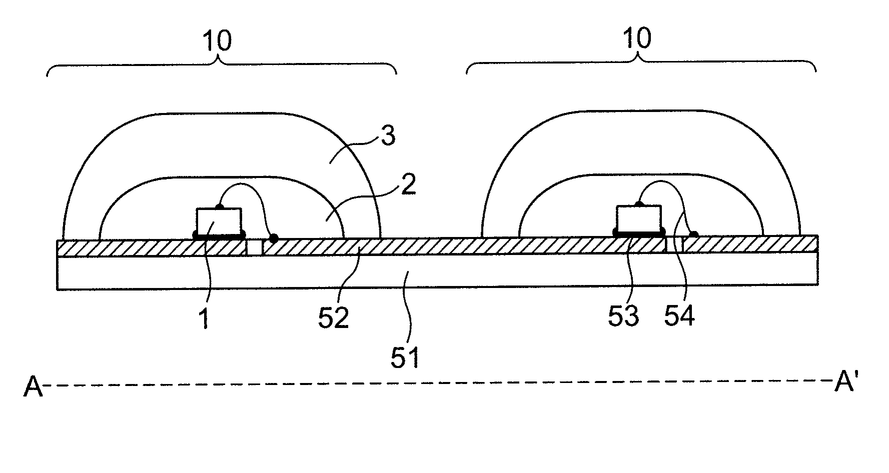
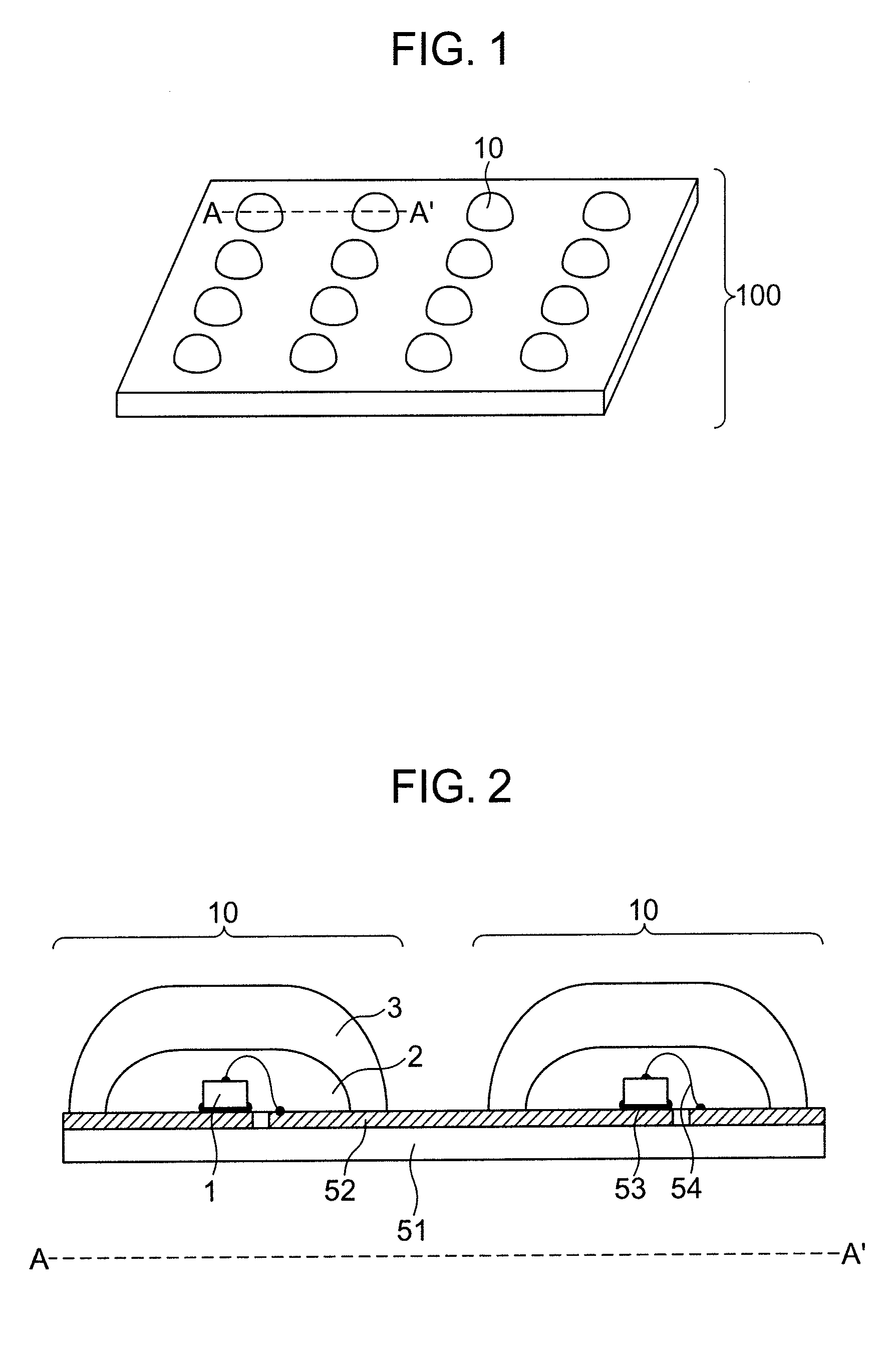
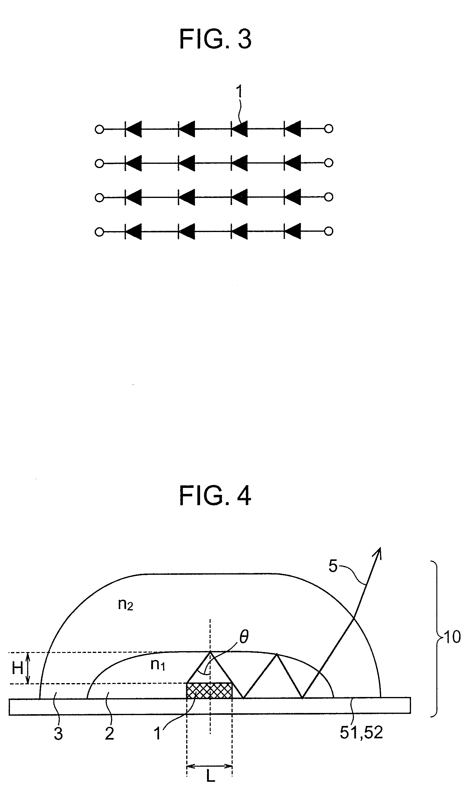
[0032]FIGS. 1 to 4, 5A to 5C, 6A, 6B, 7A, 7B and 8A to 8C are diagrams for illustrating this embodiment, in which FIG. 1 is a perspective view of an illumination device according to this embodiment, FIG. 2 is a crosssectional view taken along line A-A′ in FIG. 1, FIG. 3 is an electric circuit diagram in connection with the illumination device, FIG. 4 is a crosssectional view of a sealing structure in which travel of light is illustrated, FIGS. 5A to 5C are plan views and crosssectional views illustrating examples of the shape of a high refraction index material member in a sealing structure, FIGS. 6A and 6B are diagrams of distribution of light intensity with respect to the emergent angle in which the light intensity distribution depends on the shape of a high refractive index transparent material member, FIGS. 7A and 7B are structural diagrams of examples of light-emitting diodes, and FIG. 8A to 8C are plan views of examples of arrangements of a light-emitting diode and its periphe...

embodiment 2

[0069]FIG. 9 is a crosssectional view of a sealing structure for an illumination device according to the second embodiment of the present invention. In this embodiment, a light-emitting diode 1 is sealed by a high refractive index transparent material member 2, which is further sealed by a low refractive index material transparent member 3, as in Embodiment 1. This embodiment is different from Embodiment 1 in that the portion of the high refractive index transparent material member 2 which covers the upper surface of the light emitting member 1 has a recess above the central portion of the upper surface of the light-emitting diode 1.

[0070]Light 5 emitted by the light-emitting diode 1 emanates efficiently from the sealing structure 10 due to the high refractive index transparent material member 2 sealing the diode 1. Light 5 emitted by the light-emitting diode 1 reaches the interface between the high and low refractive index transparent material members 2 and 3. It should be particul...

embodiment 3

[0074]FIG. 11 is a crosssectional view illustrating one sealing structure for an illumination device according to this embodiment, while FIG. 12 is an electric circuit diagram in connection with the illumination device. In this embodiment, as shown in FIG. 12, sealing structures 10 are arranged in four rows in the horizontal direction and in four columns in the vertical direction, that is, as is also shown in FIG. 1.

[0075]This embodiment is similar to Embodiment 1 or 2 except the technical matters in the explanation given below. The recess as in Embodiment 2 is not particularly shown. The distinguishable points in this embodiment are that a plurality of light-emitting diodes 1 are sealed by a high refractive index transparent material member 2 and the member 2 is further sealed by a low refractive index transparent material member 3 in each sealing structure 10.

[0076]In this embodiment, the low refractive index transparent material member 3 is formed in a cylindrical shape by inject...


PUM


Abstract

An illumination device has a plurality of sealing structures each including a light-emitting diode, sealed by a high refractive index transparent material member which is further sealed by a low refractive index transparent material member. To increase a divergence angle of light radiation, the portion of the high refractive index transparent material member which covers an upper surface of the light-emitting diode is structured so as to satisfy a relation H>(L/2)/tan { sin−1(n1/n2)}, where H represents a thickness of the high refractive index transparent material member measured at the central portion of the upper surface of the light-emitting diode, L represents the length of one side of the upper surface of the light-emitting diode, n1 represents the refractive index of the high refractive index transparent material member and n2 represents the refractive index of the low refractive index transparent material member.

Description

BACKGROUND OF THE INVENTION[0001]The present invention relates to illumination devices using a light-emitting diode and to display devices in which such illumination device is used as a backlight source for a non-luminous display panel.[0002]With the recent improvement of the light emission efficiency of light-emitting diodes, light sources in various kinds of illumination devices have been changed from lamps or fluorescent lamps to light-emitting diodes. This is because the light-emitting diodes are meritorious in many points, that is, they are smaller in size, are capable of multi-colored light emission, are easily controllable, consume smaller electric power, and so forth. However, the light output and the efficiency of the light-emitting diode are not enough for illumination use in which a large light output is required or for display use in which an illumination device is used as a backlight source of a display panel. Thus, it is required to further increase the output light by...

Claims


Application Information

Patent Timeline
IPC IPC(8): F21V5/00H01L33/54H01L33/56H01L33/60H01L33/62
CPCF21K9/00G02F1/133603G02F2001/133612H01L33/56G02B19/0066H01L2224/48091G02B19/0014H01L2224/73265H01L2224/45144H01L2924/00014H01L2924/00G02F1/133612
Inventor KANEKO, HIROKITANAKA, TOSHIAKIHIYAMA, IKUOSASAKI, HIROSHISEKIGUCHI, YOSHIFUMI
Owner PANASONIC LIQUID CRYSTAL DISPLAY CO LTD
Why Eureka
Try Eureka