Semiconductor photoelectric cathode and phototube using the same semiconductor photoelctric cathode

A photocathode and semiconductor technology, applied in discharge tubes that do not contain gas ionization, photoemission cathodes, cathode ray tubes/electron beam tubes, etc., can solve problems such as difficult electron extraction

Inactive Publication Date: 2004-09-08
HAMAMATSU PHOTONICS KK
View PDF2 Cites 2 Cited by
  • Summary
  • Abstract
  • Description
  • Claims
  • Application Information

AI Technical Summary

Problems solved by technology

Therefore, even if electrons are generated in the light-absorbing layer, it is difficult to extract the electrons to the outside.

Method used


Image

  • Semiconductor photoelectric cathode and phototube using the same semiconductor photoelctric cathode
  • Semiconductor photoelectric cathode and phototube using the same semiconductor photoelctric cathode
  • Semiconductor photoelectric cathode and phototube using the same semiconductor photoelctric cathode

Examples


Embodiment Construction

[0028] Hereinafter, preferred embodiments of the present invention will be described in detail with reference to the drawings. In addition, the same symbols are used for the same elements, and overlapping descriptions are omitted.

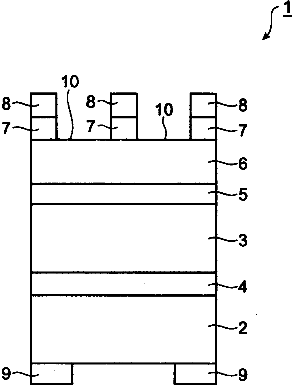
[0029] figure 1 is a diagram showing a semiconductor photocathode according to a first embodiment of the present invention. The semiconductor photocathode 1 shown in the figure has a p + Type semiconductor substrate 2, and the p formed of InAsSb - Type of light absorbing layer 3 .

[0030] Between the semiconductor substrate 2 and the light-absorbing layer 3, there is formed a p layer composed of AlGaSb having a larger energy band width than the light-absorbing layer 3 + Type hole region layer 4.

[0031] In addition, on the light absorbing layer 3, a p layer composed of AlGaSb is formed - Type hole region layer 5; on the hole region layer 5, a p layer composed of GaSb is formed - type of electron emission layer 6 .

[0032] On the electro...


PUM


Abstract

A semiconductor photocathode 1 has a p+ type semiconductor substrate 2 made of GaSb and a p- type light absorption layer 3 made of InAsSb. A p+ type hole block layer 4 with an energy band gap larger than the light absorption layer 3 and made of AlGaSb is formed between the semiconductor substrate 2 and the light absorption layer 3. A p- type hole block layer 5 made of AlGaSb is formed on the light absorption layer 3, and a p- type electron emission layer 6 made of GaSb is formed on the hole block layer 5. An n+ type contact layer 7 made of GaSb is formed on the electron emission layer 6, and pn junction is formed with the contact layer 7 and the electron emission layer 6.

Description

technical field [0001] The present invention relates to a semiconductor photocathode that emits photoelectrons upon incident photons, and a phototube using the semiconductor photocathode. Background technique [0002] Generally, the limit on the long-wavelength side of the light-receiving sensitivity wavelength of a semiconductor photocathode is almost determined by the band width of the semiconductor forming the light-absorbing layer. For example, in the case of lattice matching on an InP substrate, the limit is about 1.7 μm. [0003] In contrast, a photocathode in which a graded buffer layer in which the As-P composition is changed stepwise is provided on an InP substrate has been disclosed (Japanese Patent Laid-Open No. 11-297191). Using this photocathode can alleviate the lattice mismatch between the InP substrate and the InGaAs light absorbing layer with an In composition of 0.53 or more that belongs to the lattice mismatch series wit...

Claims


Application Information

Patent Timeline
Patent Type & Authority Applications(China)
IPC IPC(8): H01J1/34H01J29/38H01J31/50H01J40/06H01J43/08H01L29/12
CPCH01J40/06H01J1/34
Inventor 枝村忠孝新垣实
Owner HAMAMATSU PHOTONICS KK
Why Eureka
Try Eureka