
Electron tube

a technology of electron tubes and electron tubes, applied in the field of electron tubes, can solve the problems of insufficient sensitivity in the ultraviolet range of an electron tube using this, and the compound semiconductor has not been applied to a semiconductor photocathode, and achieve the effects of reducing crystal defects, high sensitivity, and reducing crystal defects

Inactive Publication Date: 2007-08-02
HAMAMATSU PHOTONICS KK
View PDF8 Cites 24 Cited by
  • Summary
  • Abstract
  • Description
  • Claims
  • Application Information

AI Technical Summary

Benefits of technology

[0005] However, such a compound semiconductor has not been applied to a semiconductor photocathode due to its many crystal defects although it has been known as a material of a photodiode or laser diode. In conventional semiconductor photocathodes, GaAs and the like are used, and the sensitivity in the ultraviolet range of an electron tube using this is not sufficient. Therefore, the inventors of this invention ap

Problems solved by technology

However, such a compound semiconductor has not been applied to a semiconductor photocathode due to its many crystal defects although it has been known as a material of a photodiode or laser diode.
In conventional semiconductor photocathodes, GaAs and the like are used, and the sensitivity in the ultraviolet range of an electron tube using this is not sufficient.

Method used


Image

  • Electron tube
  • Electron tube
  • Electron tube

Examples


Embodiment Construction

[0031] Hereinafter, an electron tube relating to an embodiment is described. The same symbol is used for components identical to each other, and overlapping description is omitted.

[0032]FIG. 20A is a cross sectional view of a side-on type photo multiplier (electron tube) 100.

[0033] The electron tube 100 comprises a vacuum container 101, a photocathode 102, and an anode 103. The vacuum container 101 is made of a glass bulb that provides an environment with an extra-low pressure inside, and its side wall forms an entrance window 101w. Light entering the inside of the vacuum container 101 via the entrance window 101w penetrates a mesh grid 104 and enters the photocathode 102. This photocathode 102 is a reflecting type photocathode, and emits photoelectrons in vacuum according to light entering.

[0034] Photoelectrons that have exited from the photocathode 102 enter a plurality of dynodes 105a, 105b, 105c, 105d, 105e, 105f, 105g, 105h, and 105i in order, and are finally collected by th...


PUM


Abstract

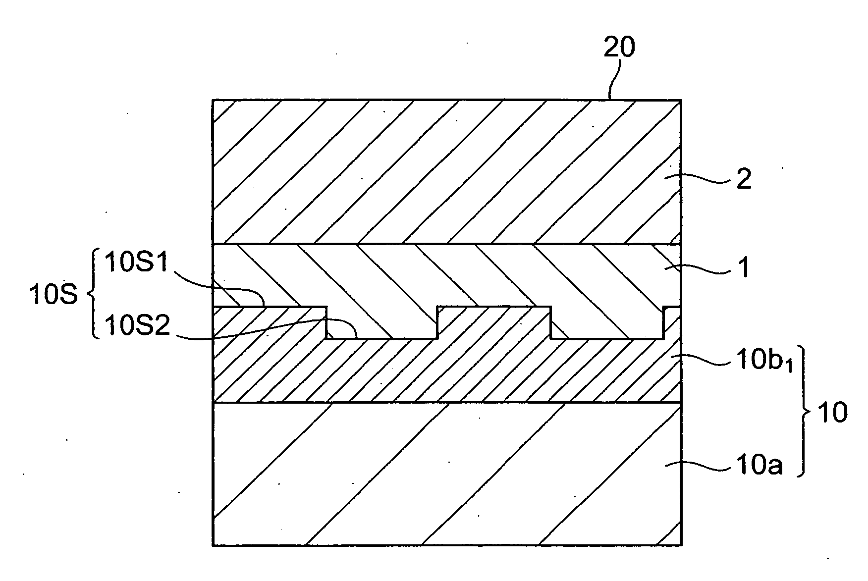
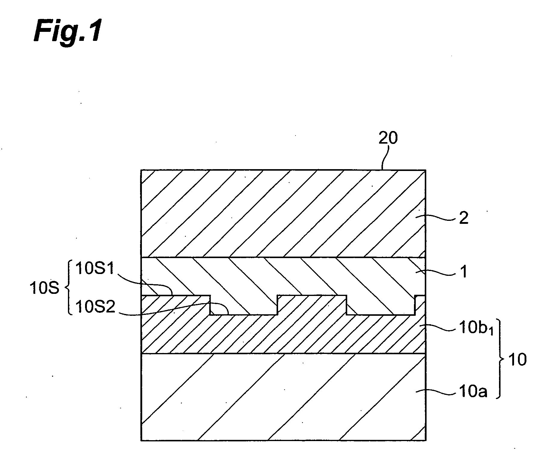
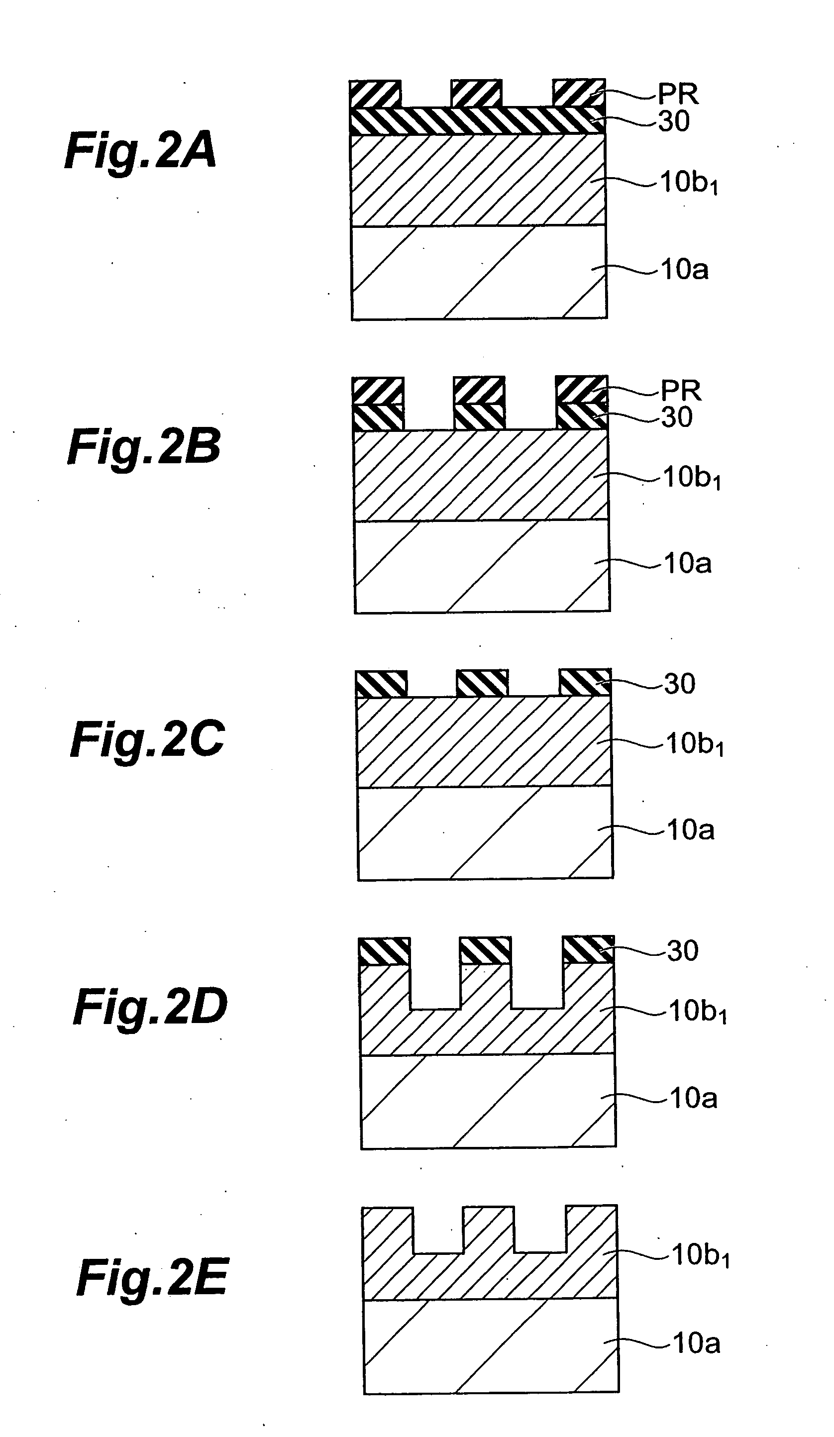
A GaN-based semiconductor photocathode is applied to an electron tube. A GaN-based compound semiconductor layer is laterally grown on a substrate, and incorporated in the electron tube. The crystal defects of the compound semiconductor layer are reduced, whereby an electron tube which has inconceivably high sensitivity is realized.

Description

BACKGROUND OF THE INVENTION [0001] 1. Field of the Invention [0002] The present invention relates to an electron tube. [0003] 2. Related Background of the Invention [0004] Conventionally, a PIN-photodiode formed by growing a GaN layer on a sapphire substrate is generally known (Japanese Published Unexamined Patent Application No. 2002-208722). In addition, a technique to form a laser diode on a GaN layer grown on a GaN substrate is also known (Japanese Published Unexamined Patent Application No. 2000-244061). In a reflecting type GaN photocathode, the relationship between the Mg doping amount and sensitivity has been studied (F. S. Shahedipour, et. al. IEEE J. Quantum Electron., 38, 333 (2002)). SUMMARY OF THE INVENTION [0005] However, such a compound semiconductor has not been applied to a semiconductor photocathode due to its many crystal defects although it has been known as a material of a photodiode or laser diode. In conventional semiconductor photocathodes, GaAs and the like ...

Claims


Application Information

Patent Timeline
IPC IPC(8): H01L29/06
CPCH01J1/34H01J40/06H01J31/50
Inventor UCHIYAMA, SHOICHITAKAGI, YASUFUMIYOSHIDA, HARUMASA
Owner HAMAMATSU PHOTONICS KK
Learn More