
Manufacturing method and apparatus for manufacturing silicon carbide epitaxial wafer

a manufacturing method and epitaxial wafer technology, applied in the direction of crystal growth process, cleaning of hollow articles, chemically reactive gases, etc., can solve the problems of easy formation of silicon carbide particles, generating leak current, and structural brittleness of attached silicon carbide, so as to reduce crystal defects

Active Publication Date: 2017-02-09
MITSUBISHI ELECTRIC CORP
View PDF4 Cites 0 Cited by
  • Summary
  • Abstract
  • Description
  • Claims
  • Application Information

AI Technical Summary

Benefits of technology

The present invention provides a method and apparatus for manufacturing silicon carbide epitaxial wafers with reduced crystal defects while avoiding damage to the growth furnace and wafer holder. This is achieved by introducing a cleaning gas with high fluid energy into the growth furnace. The technical effects include improved quality of the manufactured wafers and reduced production costs.

Problems solved by technology

If the silicon carbide epitaxial wafer has defects, the silicon carbide semiconductor device locally fails to hold a high voltage, resulting in generation of a leak current.
The attached silicon carbide is structurally brittle and can therefore form silicon carbide particles easily.
If silicon carbide particles are attached to the wafer surface, crystal defects such as downfalls and triangular defects are generated starting from the attachment points.
In the case of the method disclosed in Japanese Patent No. 5542560, not only the attached silicon carbide but also the silicon carbide film formed as protective film on internal members of the growth furnace and the wafer holder is etched and it is, therefore, difficult to perform cleaning management.
Also, special expelling equipment is required to enable use of chlorine trifluoride, for example, because it corrodes the apparatus and piping.
The method thus entails problems in terms of operation and cost.
Further, because the rate of etching of silicon carbide is lower than that of etching of silicon, a long time is taken to complete cleaning and it is difficult to completely remove silicon carbide.
In the case of the method disclosed in Japanese Patent Laid-Open No. 2014-154865, iodine heptafluoride, which does not etch graphite, is used but the silicon carbide film formed as protective film on the wafer holder and internal members of the growth furnace are thereby etched, as in the case of the method disclosed in Japanese Patent No. 5542560, and it is difficult to perform cleaning management.
Thus, use of a fluorine-based gas as cleaning gas entails the problem of members other than the attached silicon carbide being etched.

Method used


Image

  • Manufacturing method and apparatus for manufacturing silicon carbide epitaxial wafer
  • Manufacturing method and apparatus for manufacturing silicon carbide epitaxial wafer
  • Manufacturing method and apparatus for manufacturing silicon carbide epitaxial wafer

Examples


first embodiment

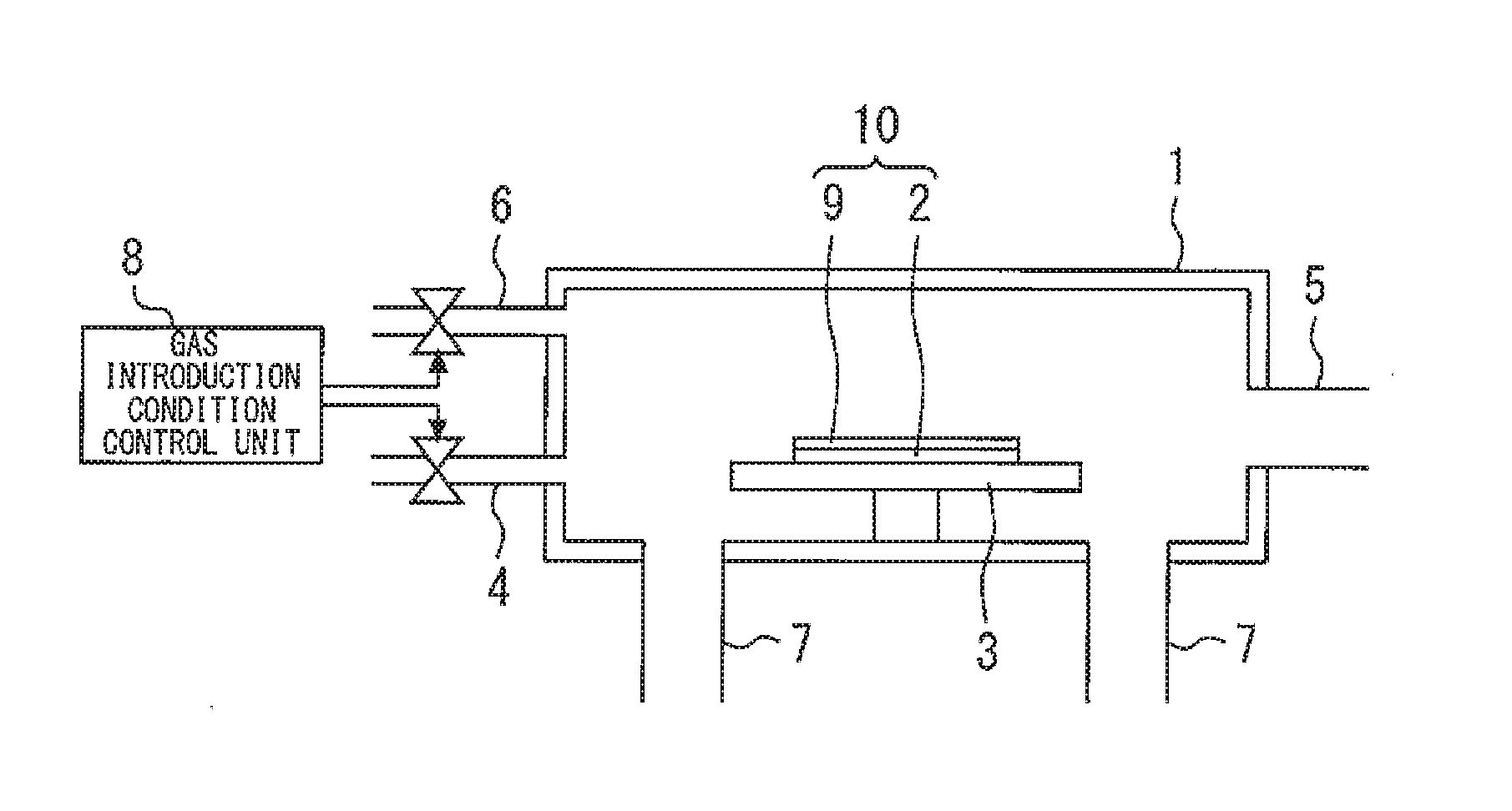
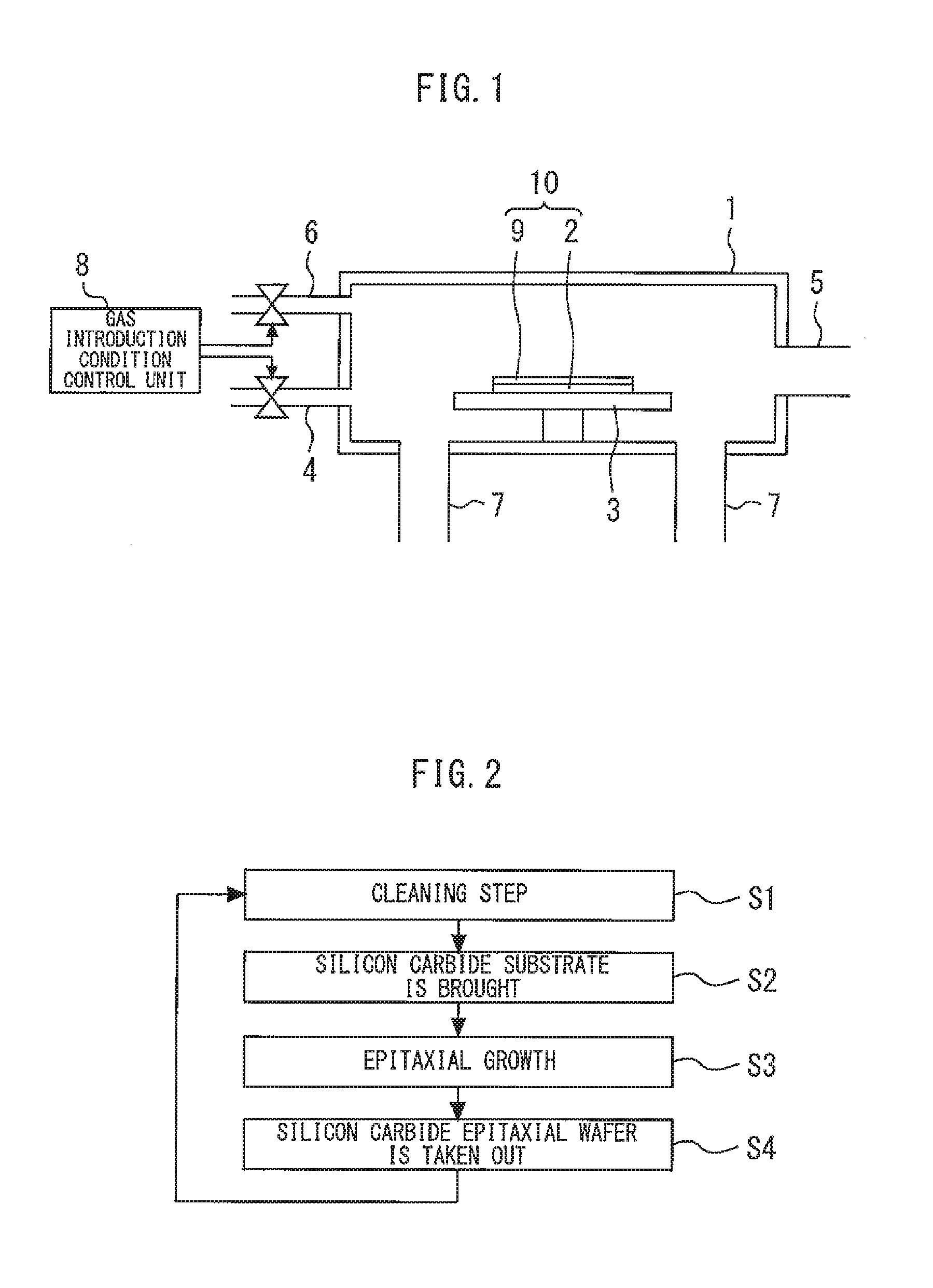
[0019]FIG. 1 is a sectional view of an apparatus for manufacturing a silicon carbide epitaxial wafer according to a first embodiment of the present invention. A wafer holder 3 on which a silicon carbide substrate 2 is mounted is provided in a growth furnace 1 (epitaxial growth furnace) in which epitaxial growth is performed. A processing gas introduction port 4 introduces a processing gas including a carrier gas and a raw-material gas into the growth furnace 1 in an epitaxial growth step. A processing gas exhaust port 5 discharges from the growth furnace 1 the processing gas introduced through the processing gas introduction port 4.

[0020]A cleaning gas introduction port 6 introduces, into the growth furnace 1, in a cleaning step, a cleaning gas for removing silicon carbide in polycrystalline form of dendrite-like structure attached to inner wall surfaces of the growth furnace 1. Gas exhaust ports 7 discharge from the growth furnace 1 the cleaning gas introduced through the cleaning ...

second embodiment

[0031]FIG. 4 is a flowchart showing a silicon carbide epitaxial wafer manufacturing process according to a second embodiment of the present invention. The same manufacturing apparatus as that in the first embodiment is used for the manufacturing process in the second embodiment.

[0032]First, a cleaning step (step S1), a silicon carbide substrate 2 transport step (step S2) and an epitaxial growth step (step S3) are carried out, as those in the first embodiment, thereby forming the silicon carbide epitaxial wafer 10. These steps are the same as those in the first embodiment and detailed descriptions of them will not be repeated. After silicon carbide in polycrystalline form of dendrite-like structure attached to the inner wall surfaces of the growth furnace 1 and the wafer holder 3 is removed in the cleaning step (step S1), the epitaxial growth step (step S3) is executed. Therefore, substantially no silicon carbide particles are generated in the epitaxial growth step. The silicon carbi...


PUM

PropertyMeasurementUnit
fluid energyaaaaaaaaaa

Abstract

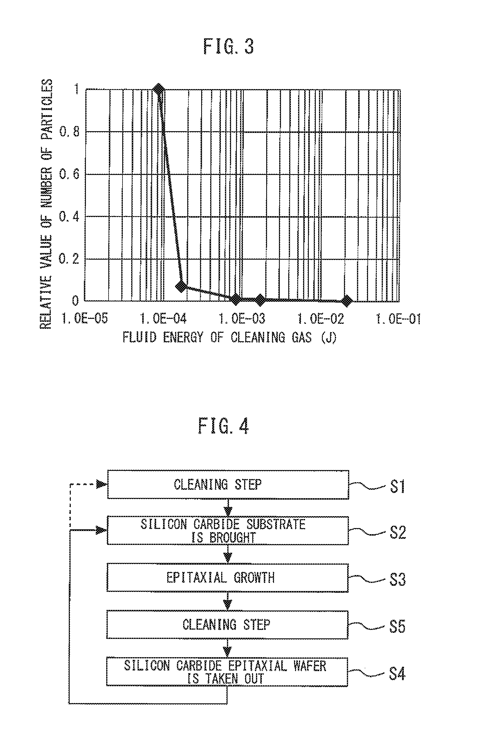
A manufacturing method for manufacturing a silicon carbide epitaxial wafer includes: introducing a cleaning gas into a growth furnace to remove dendrite-like polycrystal of silicon carbide attached to an inner wall of the growth furnace; after introducing the cleaning gas, bringing a silicon carbide substrate in the growth furnace; and growing a silicon carbide epitaxial layer on the silicon carbide substrate by introducing a processing gas into the growth furnace to manufacture a silicon carbide epitaxial wafer, wherein the cleaning gas having fluid energy of 1.6E−4 [J] or higher is introduced into the growth furnace.

Description

BACKGROUND OF THE INVENTIONField of the Invention[0001]The present invention relates to a manufacturing method and apparatus for manufacturing a silicon carbide epitaxial wafer.Background Art[0002]In recent years, a silicon carbide (hereinafter referred to as SiC) semiconductor has attracted attention mainly as a material for power devices for power control because its bandgap, dielectric breakdown electric field intensity, saturated drift speed and thermal conductivity are higher than those of silicon semiconductors. In fact, a power device using the SiC semiconductor is capable of largely reducing power loss, being reduced in size and realizing energy saving at the time of power supply power conversion and can therefore be a key device for, for example, improving the performance of electric vehicles and improving the functions of solar battery systems or the like in realization of a low-carbon society.[0003]In making a SiC power device, a layer to be provided as an active region o...

Claims


Application Information

Patent Timeline
Patent Type & Authority Applications(United States)
IPC IPC(8): H01L21/02C23C16/44B08B9/093C23C16/455
CPCH01L21/02529H01L21/02378B08B9/093C23C16/455C23C16/4412H01L21/0262C30B25/14C30B25/20C30B25/00C23C16/4405C30B29/36C11D2111/20
Inventor OHNO, AKIHITOSAKAI, MASASHIMITANI, YOICHIROYAMAMOTO, TAKAHIROKIMURA, YASUHIROMIZOBE, TAKUMATOMITA, NOBUYUKI
Owner MITSUBISHI ELECTRIC CORP
Learn More