

Magnetic RAM using magnetic resistance effect to store information
A technology of random access memory and storage unit, which is applied to devices applying electro-magnetic effects, static memory, digital memory information, etc., and can solve problems such as increased current consumption and increased bit line current
- Summary
- Abstract
- Description
- Claims
- Application Information
AI Technical Summary
Problems solved by technology
Method used
Image

Examples
Embodiment approach 1
[0039] First, the MRAM according to Embodiment 1 of the present invention will be described.
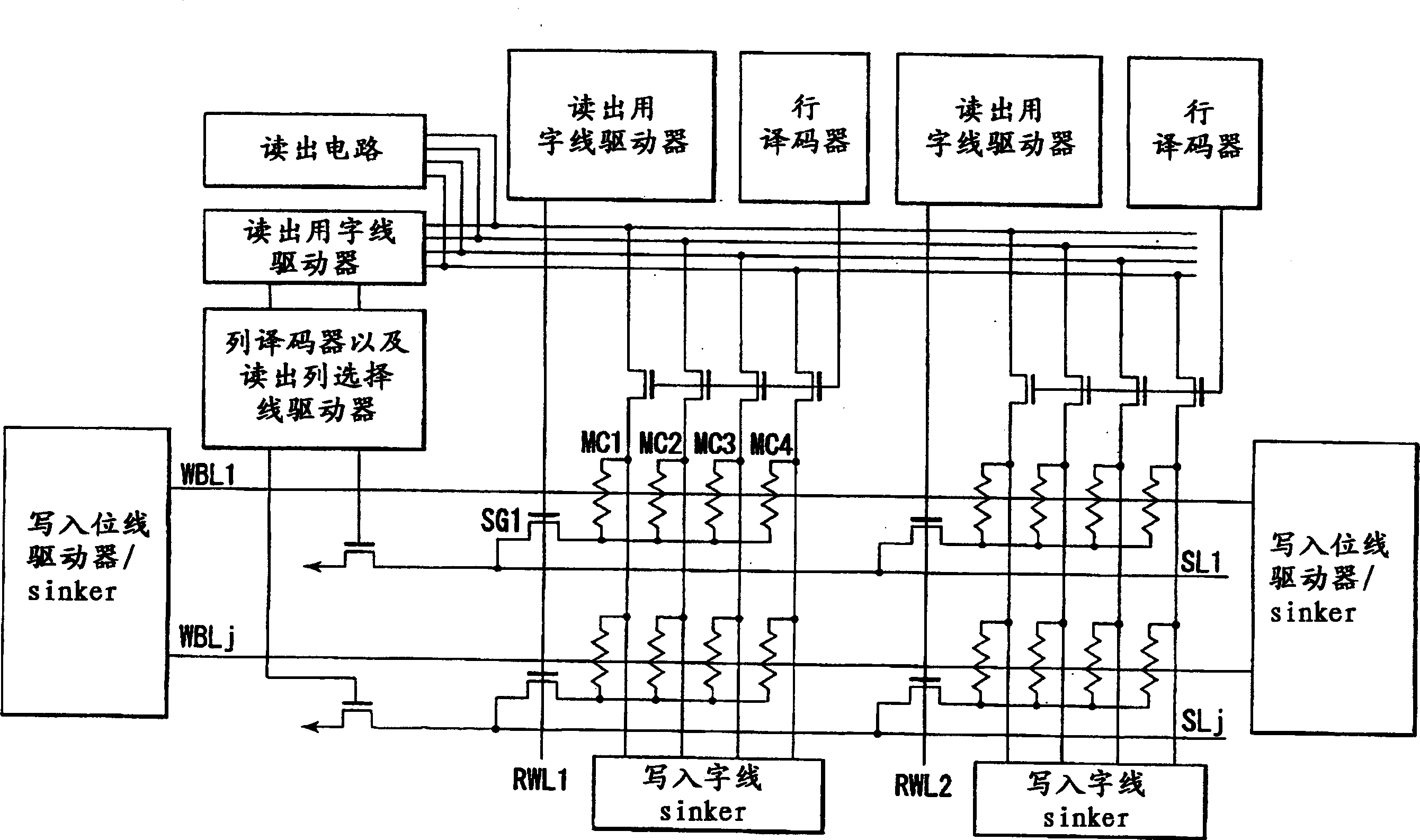
[0040] Figure 5 It is a circuit diagram showing the configuration of the MRAM in the first embodiment.
[0041] Such as Figure 5 As shown, cross-point memory cells MC1, MC2, ... MC4 constituted by MTJ elements have one end connected to sub bit line SBL1 as a common node. The sub bit line SBL1 is connected to the main bit line MBL1 using the select metal oxide semiconductor transistor SG1 as a switch. A signal line SS1 is connected to the gate of the selection MOS transistor SG1 , and the signal line SS1 is connected to the row decoder 11 . One end of main bit line MBL1 is connected to sense amplifier (S / A) 12 via column gate circuit CG1.
[0042] To the other ends of the memory cells MC1 , MC2 , . . . , MC4 , lines L1 , L2 , . . . , L4 are respectively connected. A bit line driver / sinker circuit 13 for writing is connected to one end of the lines L1 to L4. The other ends of t...
Embodiment approach 2
[0066] Hereinafter, the MRAM according to Embodiment 2 of the present invention will be described.
[0067] Figure 8 It is a circuit diagram showing the configuration of the MRAM of the second embodiment. Figure 5 The difference between Embodiment 1 and Embodiment 2 shown above is that, while Embodiment 1 stores 1-bit information in 1 memory cell, Embodiment 2 has 1-bit information stored in 2 memory cells ( So-called 2 bits / unit) configuration. The same reference numerals are assigned to the same components as those in the first embodiment described above, and their descriptions will be omitted, and only the different components will be described below.
[0068] Such as Figure 8 As shown, the gates of the column gate circuits CG1 and CG2 are commonly connected to the signal line SC1. Other circuit configurations are the same as those in the first embodiment described above.
[0069] The operation of the MRAM according to Embodiment 2 is as follows.
[0070] During re...
Embodiment approach 3
[0077] Hereinafter, an MRAM according to Embodiment 3 of the present invention will be described.
[0078] Figure 10 It is a circuit diagram showing the configuration of the MRAM of the third embodiment. In Embodiment 2 described above, writing of complementary data requires two write cycles, but in Embodiment 3, writing of complementary data can be completed in one write cycle.
[0079] In the second embodiment described above, the signal line SS1 is connected to the gates of the selective metal oxide semiconductor transistors SG1 and SG2, but in the third embodiment, the signal line SS1 is connected to the gates of the selective metal oxide semiconductor transistors SG1 and SG3. top notch. Furthermore, in the second embodiment described above, one end of the current path of the selective metal oxide semiconductor transistor SG3 is connected to the main bit line MBL1, and one end of the current path of the selective metal oxide semiconductor transistor SG4 is connected to ...
PUM
 Abstract
Description
Claims
Application Information