Solid state image sensing apparatus with enhanced sensitivity realized by improving linear characteristic of photodiode and its driving method

A solid-state imaging device and photodiode technology, which is applied to electric solid-state devices, radiation control devices, components of color TVs, etc., can solve the problem that the saturated signal charge Qs cannot be overestimated, and can suppress blurring and expand linearity. The effect of improved range and sensitivity

Inactive Publication Date: 2004-11-03
PANASONIC CORP
View PDF1 Cites 0 Cited by
  • Summary
  • Abstract
  • Description
  • Claims
  • Application Information

AI Technical Summary

Problems solved by technology

The second bias period is the invalid data output period starting from the exposure period in the same figure, but at least includes the second field output period.
[0019] However, in the prior art, when the substrate bias modulation is performed before the end of the exposure, it can be estimated that the decrease will increase the saturation signal charge Qs that decreases with time when the mechanical shutter blocks light. To prevent blurring during this period, it is necessary to pre-set the height of the overflow barrier OFB according to the second bias voltage to be lower than the potential barrier of the readout gate, and there is a limit on the amount of bias voltage modulation
Therefore, the increase in the saturation signal charge Qs cannot be overestimated

Method used


Image

  • Solid state image sensing apparatus with enhanced sensitivity realized by improving linear characteristic of photodiode and its driving method
  • Solid state image sensing apparatus with enhanced sensitivity realized by improving linear characteristic of photodiode and its driving method
  • Solid state image sensing apparatus with enhanced sensitivity realized by improving linear characteristic of photodiode and its driving method

Examples


Embodiment Construction

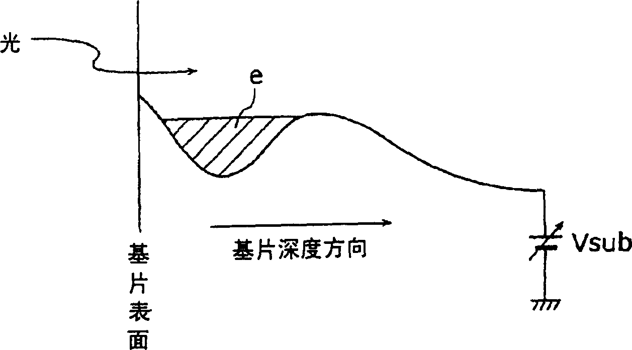
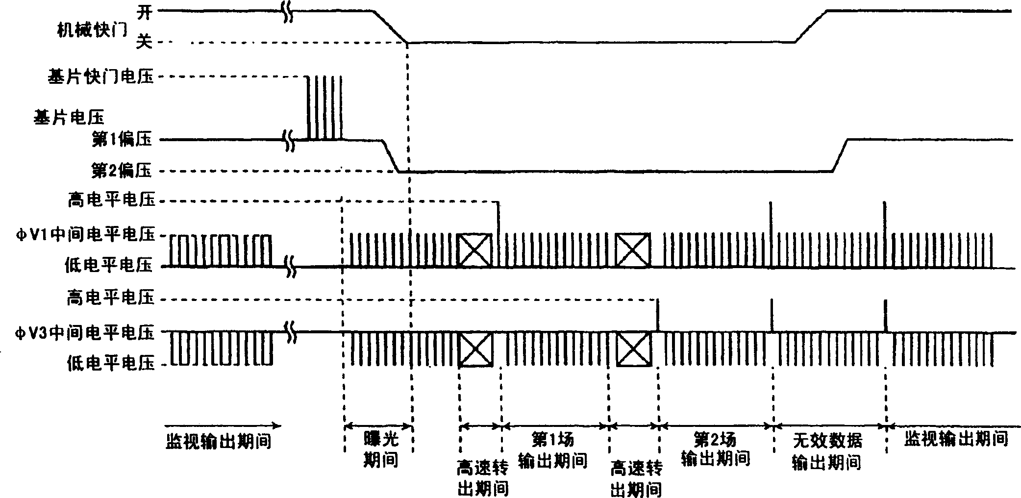
[0064] The solid-state imaging device in the embodiment of the present invention is characterized in that (A) at the start of the exposure period (see Figure 7 T3~T4) Set the barrier height of the overflow barrier OFB to be higher than the potential barrier of the readout gate (refer to Figure 12A ), (B) In addition, after the exposure period is completed and before the vertical CCD is rotated out at high speed (refer to Figure 7 T5), temporarily reduce the barrier height of the overflow barrier OFB, and transfer the excess charge to the substrate (refer to Figure 13 , Figure 14 ). Thereby, the linearity characteristic of the photodiode is improved to increase the sensitivity.

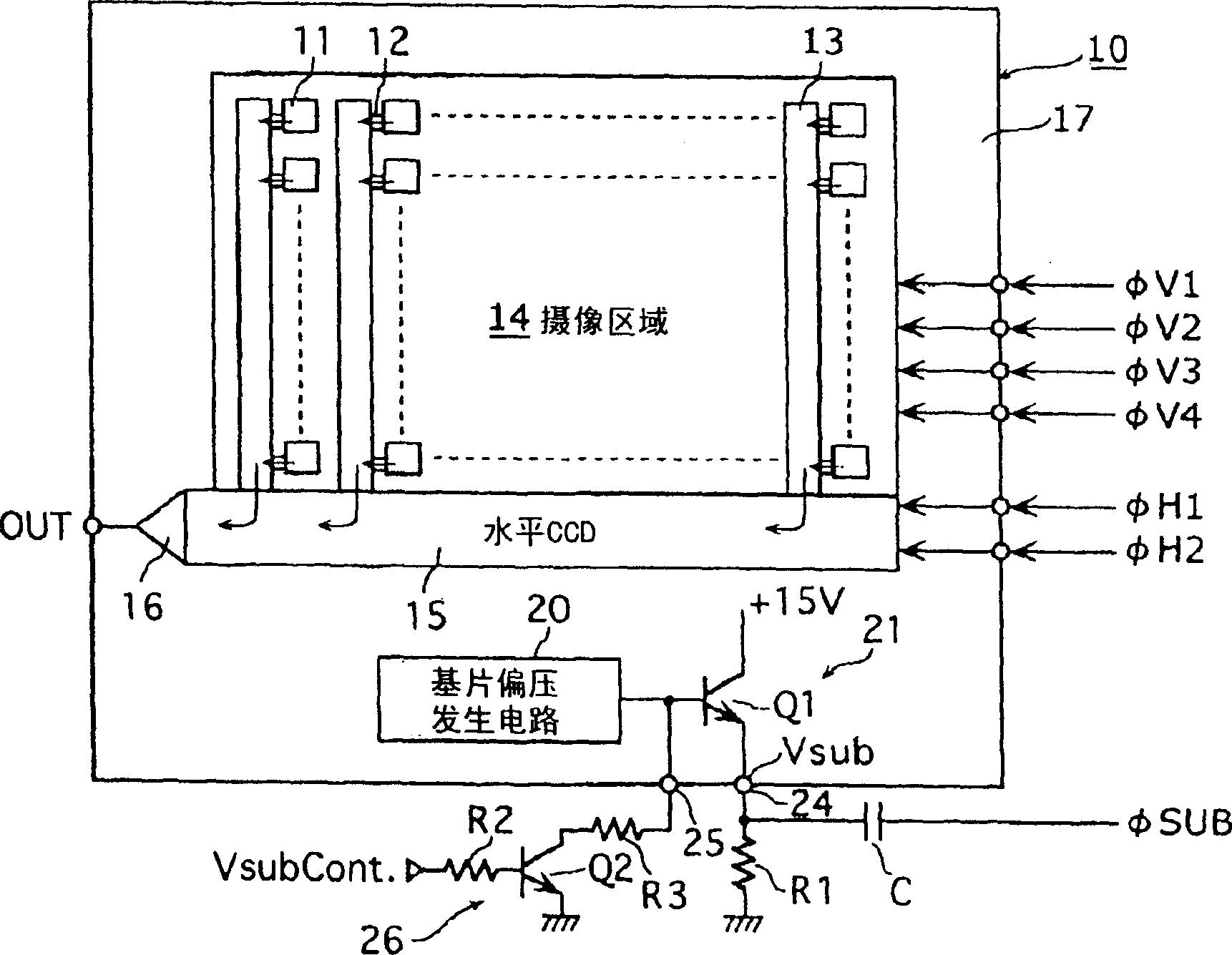
[0065] Figure 4 It is a block diagram showing a schematic configuration of the solid-state imaging device in the embodiment of the present invention. The solid-state imaging device 1 includes a lens 2 , a mechanical shutter 3 , a drive unit 4 , a signal processing unit 5 , and a solid-state ...


PUM


Abstract

The driver unit of the solid state image sensing apparatus of the present invention changes the substrate bias voltage from the first bias voltage to the second voltage which is lower than the first bias voltage and is for making a height of the overflow barrier higher than the height of the barrier in the readout gate and lowers the height of the overflow barrier by superimposing the saturation signal control pulse on the second bias voltage after the end of the exposure period and before sweeping out all the signal charge of the vertical CCDs.

Description

technical field [0001] The invention relates to a CCD (Charge Coupled Device) solid-state imaging device adopting an overflow-drain OFD structure and a method thereof. Background technique [0002] In recent years, digital video cameras, digital video cameras, and mobile phones with video cameras have become widespread, and image sensors such as CCD imaging devices have been miniaturized along with higher resolution. [0003] figure 1 It is a block diagram showing the configuration of a conventional CCD solid-state imaging device described in Patent Document 1 and the like. exist figure 1 Among them, the solid-state imaging device 10 has a plurality of photodiodes 11, a plurality of readout gates 12, a plurality of vertical CCDs 13, a plurality of horizontal CCDs 15, an output amplifier 16, a substrate bias voltage generating circuit 20, and a transistor Q1 arranged two-dimensionally. In addition, in figure 1 In FIG. 2 , a transistor Q2 and resistors R1 to R3 are also sh...

Claims


Application Information

Patent Timeline
Patent Type & Authority Applications(China)
IPC IPC(8): H01L27/148H04N5/335H04N5/341H04N5/353H04N5/369H04N5/372
CPCH04N3/1568H04N5/3728H04N5/3592H04N25/622H04N25/73G05F3/205G05F3/24H04N25/766
Inventor 河野明启武藤信彦藤田武
Owner PANASONIC CORP
Why Eureka
Try Eureka