Measuring back-side voltage of an integrated circuit

An integrated circuit and voltage technology, which is applied in the field of measuring the back voltage of integrated circuits, to increase editing capabilities and promote reverse engineering

Inactive Publication Date: 2004-12-01
诚信系统公司
View PDF6 Cites 3 Cited by
  • Summary
  • Abstract
  • Description
  • Claims
  • Application Information

AI Technical Summary

Problems solved by technology

This method requires the labor and expense of using specialized equipment to deliver the necessary chemicals
Once the substrate is completely removed, there is still the problem of locating exactly which nodes to probe

Method used


Image

  • Measuring back-side voltage of an integrated circuit
  • Measuring back-side voltage of an integrated circuit
  • Measuring back-side voltage of an integrated circuit

Examples


Embodiment Construction

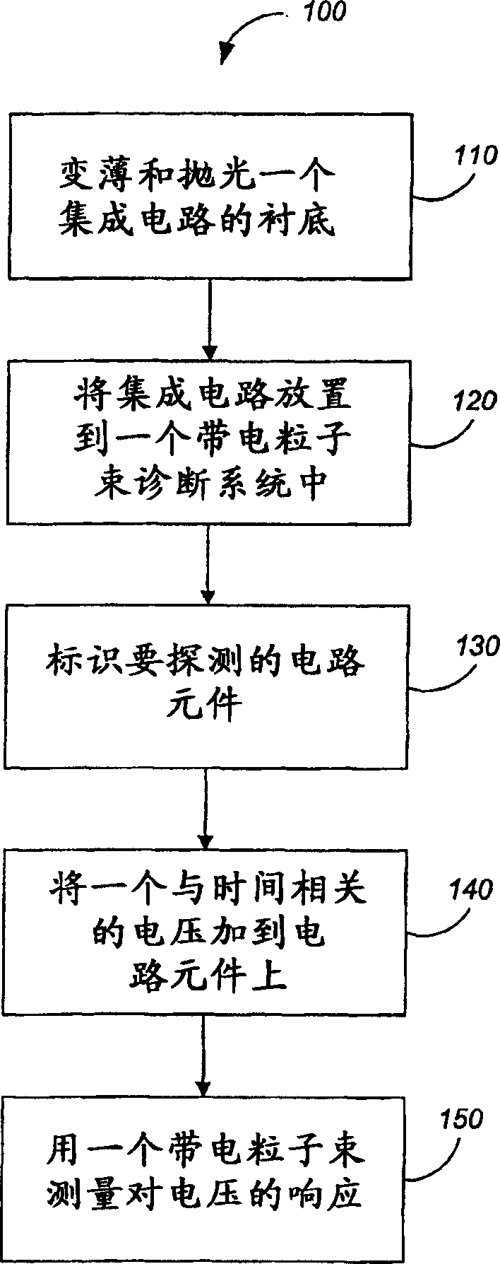
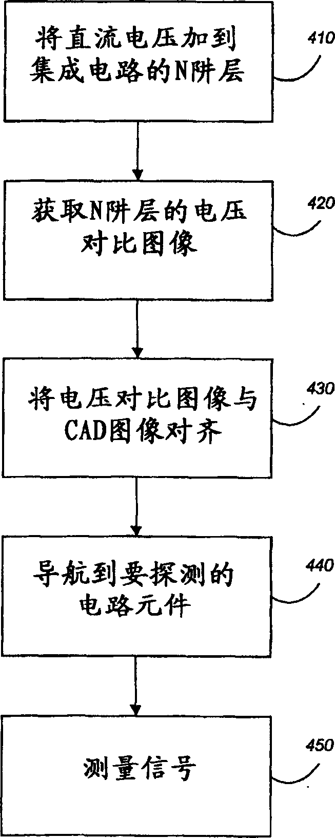
[0023] In accordance with the present invention, a charged particle beam diagnostic system can be used to diagnose, qualify or modify flip-chip or other integrated circuits by accessing underlying structures through a thinned silicon substrate. This operation can even be performed on integrated circuits that cannot be accessed in their entirety but can be accessed after sufficient disassembly, so the invention has application for failure analysis.

[0024] like figure 1 As shown, a method 100 according to the present invention has five main steps. First, refer to figure 2 As described in detail in , the substrate of an integrated circuit (eg, a flip-chip integrated circuit) is thinned and polished (step 110). like image 3 As shown, the thinned integrated circuit is placed into a charged particle flux diagnostic system (step 120). Suitable systems include the Schlumberger IDS 10000da Electron Beam Detection System available from Schlumberger Semiconductor Solutions of San...


PUM


Abstract

Methods for integrated circuit diagnosis, characterization or modification using a charged particle beam. In one implementation, the bulk silicon substrate of an integrated circuit is thinned to about 1 to 3 mum from the deepest well, a voltage is applied to a circuit element that is beneath the outer surface of the thinned substrate. The applied voltage induces an electrical potential on the outer surface, which is detected as a surface feature on the outer surface by its interaction with the charged particle beam.

Description

technical field [0001] The present invention relates to the use of charged particle beams for integrated circuit diagnosis, qualification and modification. Background technique [0002] Over the years, e-beam diagnostic systems have become powerful tools for integrated circuit (IC) qualification and debug applications. Notable aspects of electron beam diagnostic systems include secondary electron imaging, circuit navigation using embedded computer automation design (CAD) displays, and voltage measurement from active circuits using voltage contrast principles. (see eg US Patent No. 4706019). Electron beam diagnostic systems are traditionally used on the front side of integrated circuits. The implementation of face-down or flip-chip integrated circuit packaging imposes severe limitations on the use of e-beam diagnostic systems. Integrated circuits using flip-chip packaging have only the backside (silicon substrate) of the integrated circuit exposed. [0003] Three methods ...

Claims


Application Information

Patent Timeline
Patent Type & Authority Applications(China)
IPC IPC(8): G01R31/302G01R31/311H01L21/66
CPCH01L22/14G01R31/311H01L2924/014H01L2224/13H01L2924/1305H01L2924/00014H01L2924/00H01L2224/0401
Inventor 克里斯托弗·肖陶春诚西奥多·R.·朗德奎斯特
Owner 诚信系统公司
Why Eureka
Try Eureka