
Measuring back-side voltage of an integrated circuit

a backside voltage and integrated circuit technology, applied in the direction of individual semiconductor device testing, semiconductor/solid-state device testing/measurement, instruments, etc., can solve the problems of complex device design, specialized equipment, time-consuming device modification after manufacturing, and the inability to build the necessary probe points for probing, etc., to facilitate reverse engineering the ic, enhance etching, and add in-circuit editing capability

Inactive Publication Date: 2005-03-29
DCG SYST
View PDF9 Cites 10 Cited by
  • Summary
  • Abstract
  • Description
  • Claims
  • Application Information

AI Technical Summary

Benefits of technology

The invention can be implemented to realize one or more of the following advantages. 1. An IC with substantial metal on the front side can be diagnosed, characterized, or modified from the back side with a charged particle beam. 2. This can be done without damaging the circuit or making it inoperative. 3. A circuit element can be measured without manufacturing a probe point connected to the circuit element. 4. A number of circuit elements can be diagnosed at the same time by means of an imaging approach or a beam multiplexing approach. 5. A charged particle beam can image circuit elements and the image can be used to navigate the circuit and find the circuit element or elements to be probed. 6. The beam can be used to edit the circuit by injecting a charge, for example, a charge to damage a gate oxide on a CMOS transistor. 7. By using the techniques of the invention to map the transistors of an IC, one can facilitate the reverse engineering of the IC. 8. The applications of e-beam probing can be expanded because focused ion beam probe points do not necessarily have to be created. 9. In-circuit measurement and circuit modifications can be performed by the same instrument, for example, a conventional e-beam prober. 10. This will add in-circuit editing capability to e-beam systems, by means of e-beam depositions and enhanced etching. 11. Having found structures of an IC, one can use the e-beam to deliver an electron dose to any node for failure analysis using EBIC (electron beam induced current).

Problems solved by technology

The implementation of face-down or flip-chip IC packaging has created severe limitations for the use of electron beam diagnostic systems.
These approaches require either complicated device designs, specialized equipment, or time consuming device modifications after manufacturing.
The nodes that are identified for probing may not have the necessary built-in probe points due to oversight during the device design.
An alternative is to include probe points for every device node, which is impractical.
This method, while effective, can result in damage to the device by the focused ion beam system.
Furthermore, the focused ion beam system can only expose one device node at a time.
Creating access to multiple device nodes is a difficult, potentially damaging, and time-consuming process.
This approach requires the effort and expense of using specialized equipment to deliver the necessary chemical agents.
Once the substrate is completely removed, the problem of exactly locating the node of interest to be probed still remains.

Method used


Image

  • Measuring back-side voltage of an integrated circuit
  • Measuring back-side voltage of an integrated circuit
  • Measuring back-side voltage of an integrated circuit

Examples


Embodiment Construction

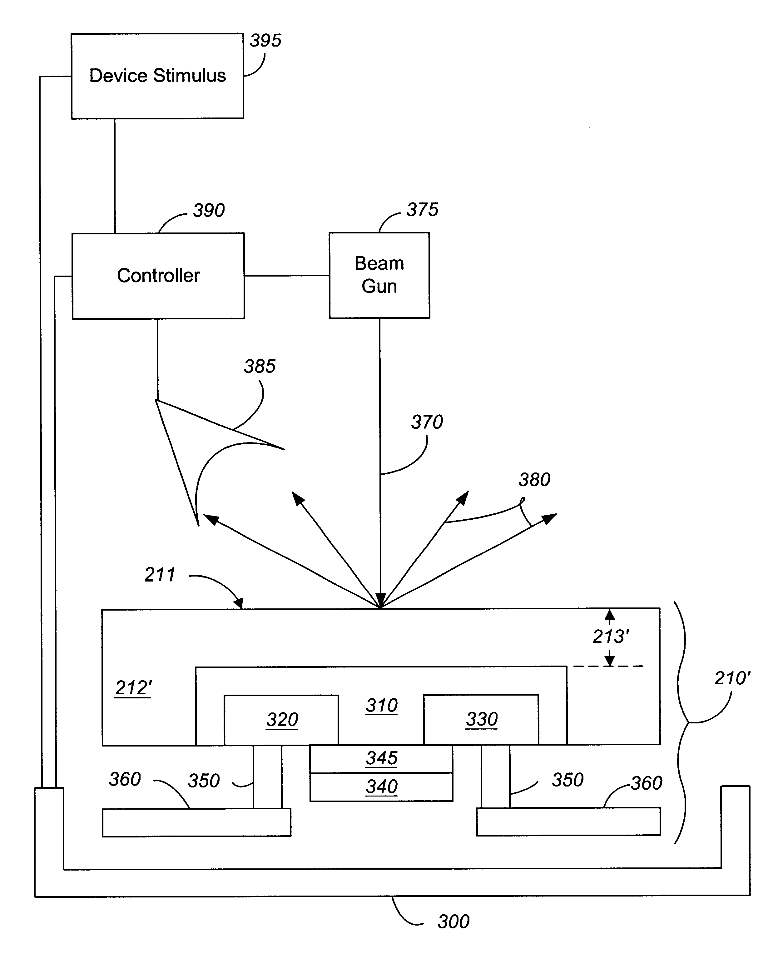
A charged particle beam diagnostic system can be used in accordance with the invention to diagnose, characterize, or modify circuit elements of a flip-chip or other IC by providing access to underlying structures through a thinned silicon substrate. This can be done even on ICs that cannot be accessed as a whole but can be accessed when sufficiently disassembled, and so the invention has application to failure analysis.

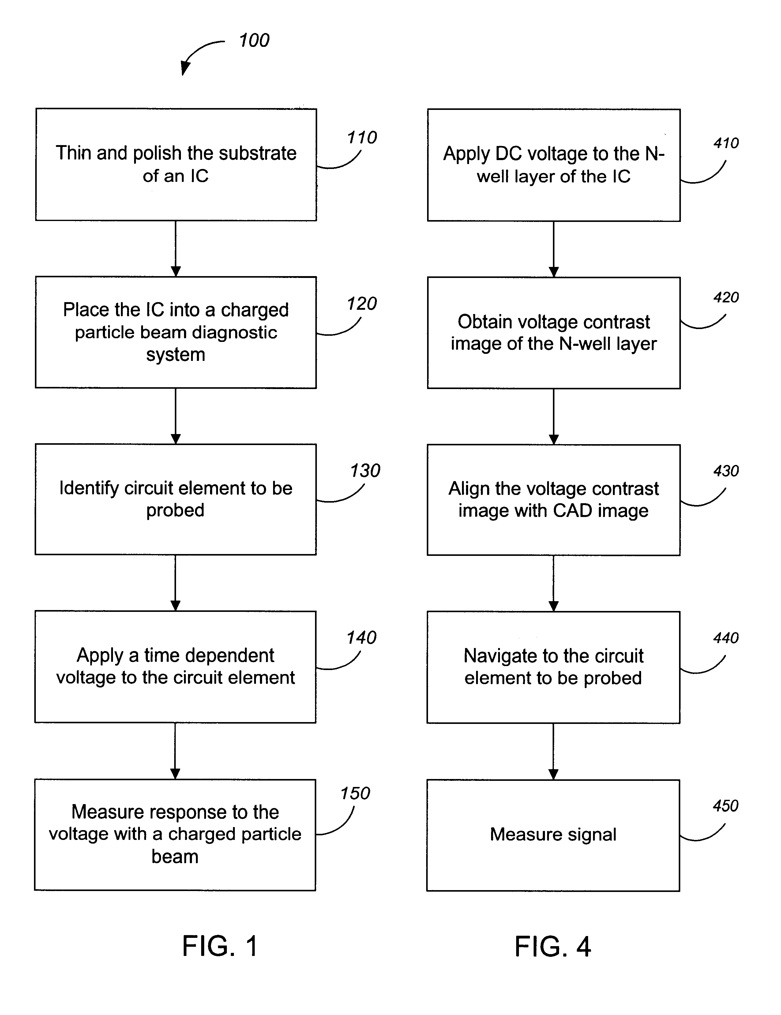
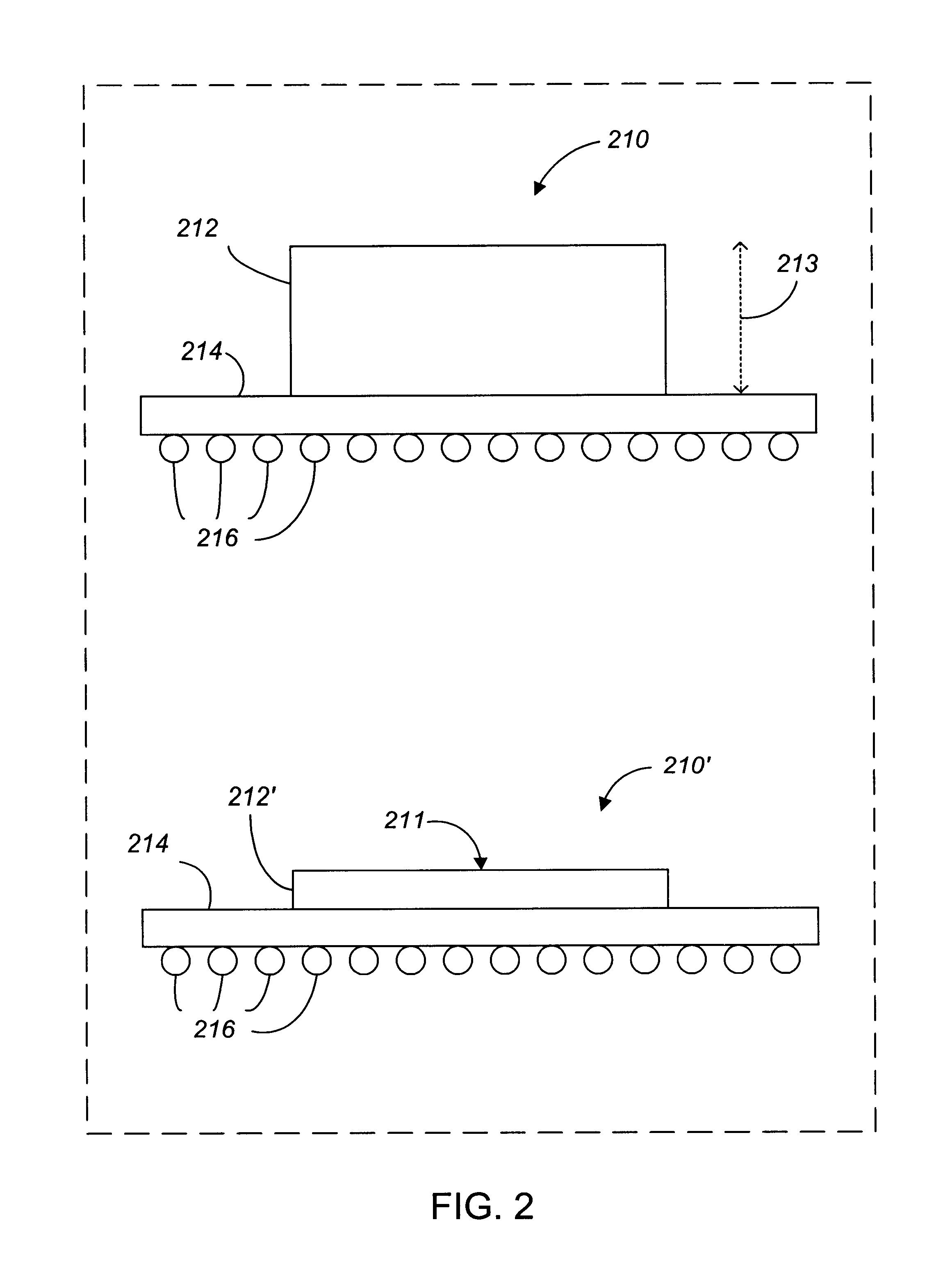
As shown in FIG. 1, one method 100 in accordance with the invention has five major steps. Preliminarily, the substrate of an IC, e.g., a flip-chip IC, is thinned and polished (step 110) as explained in more detail in reference to FIG. 2. The thinned IC is placed in a charged particle beam diagnostic system (step 120) as shown in FIG. 3. Appropriate systems include the Schlumberger IDS 10000da e-beam probe system available from Schlumberger Semiconductor Solutions of San Jose, Calif. Using this system, a circuit element to be probed is identified (step 130); an impleme...


PUM


Abstract

Methods for integrated circuit diagnosis, characterization or modification using a charged particle beam. In one implementation, the bulk silicon substrate of an integrated circuit is thinned to about 1 to 3 μm from the deepest well, a voltage is applied to a circuit element that is beneath the outer surface of the thinned substrate. The applied voltage induces an electrical potential on the outer surface, which is detected as a surface feature on the outer surface by its interaction with the charged particle beam.

Description

BACKGROUNDThis invention relates to integrated circuit diagnosis, characterization and modification using charged particle beams.Electron beam diagnostic systems have been a powerful tool for integrated circuit (IC) characterization and debug applications for many years. The well-known aspects of electron beam diagnostic systems include secondary electron imaging, circuit navigation using a built-in computer automated design (CAD) display, and voltage measurements from active circuits using voltage contrast principles. (See, for example, U.S. Pat. No. 4,706,019.) Electron beam diagnostic systems have traditionally been used on the frontside of an IC. The implementation of face-down or flip-chip IC packaging has created severe limitations for the use of electron beam diagnostic systems. An IC using flip-chip packaging has only the back-side (silicon substrate) of the IC exposed.Three approaches currently exist for making electron beam measurements on the back-side of a flip-chip devi...

Claims


Application Information

Patent Timeline
Patent Type & Authority Patents(United States)
IPC IPC(8): G01R31/28G01R31/311H01L21/66G01R31/302
CPCG01R31/311H01L22/14H01L2924/014H01L2224/13H01L2924/1305H01L2924/00H01L2924/00014H01L2224/0401
Inventor SHAW, CHRISTOPHERTSAO, CHUN-CHENGLUNDQUIST, THEODORE R.
Owner DCG SYST
Learn More