Aluminum gallium nitride/gallium nitride high electron mobility transistors having a gate contact on a gallium nitride based cap segment and methods of fabricating same

A high electron mobility, transistor technology, applied in semiconductor/solid-state device manufacturing, circuits, electrical components, etc.

Inactive Publication Date: 2004-12-08
CREE INC
View PDF3 Cites 28 Cited by
  • Summary
  • Abstract
  • Description
  • Claims
  • Application Information

AI Technical Summary

Problems solved by technology

However, this approach is not suitable for AlGaN/GaN HEMT structures, because the upper surface of GaN is gener

Method used


Image

  • Aluminum gallium nitride/gallium nitride high electron mobility transistors having a gate contact on a gallium nitride based cap segment and methods of fabricating same
  • Aluminum gallium nitride/gallium nitride high electron mobility transistors having a gate contact on a gallium nitride based cap segment and methods of fabricating same
  • Aluminum gallium nitride/gallium nitride high electron mobility transistors having a gate contact on a gallium nitride based cap segment and methods of fabricating same

Examples


Embodiment Construction

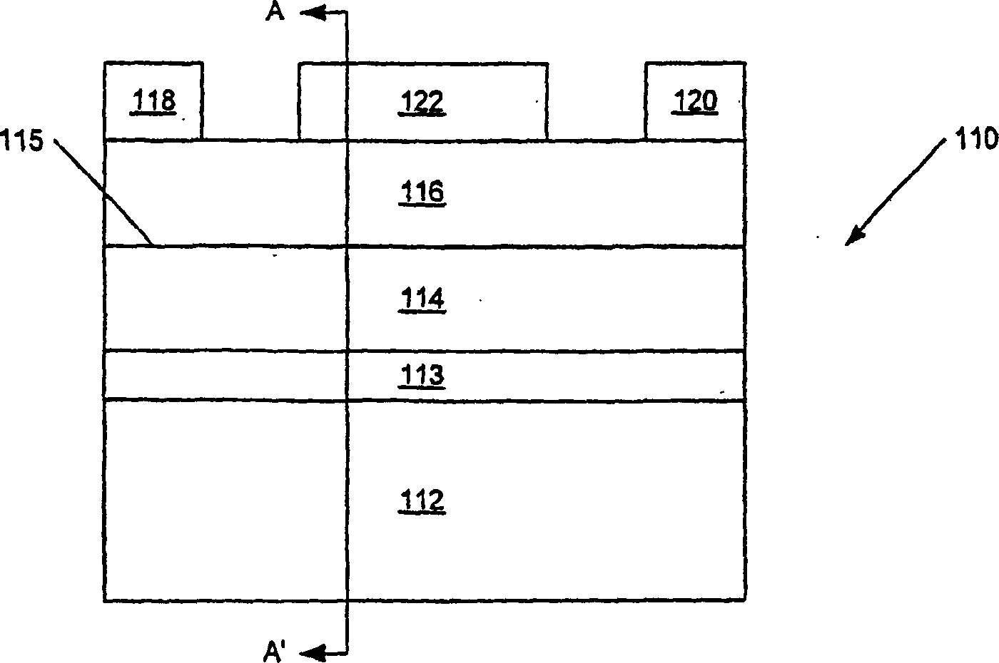
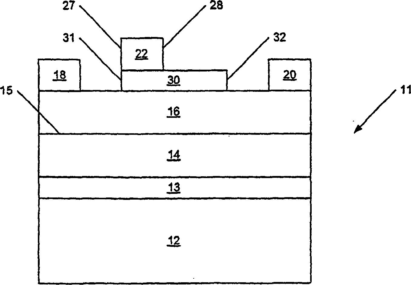
[0028]The present invention will now be described more fully with reference to the accompanying drawings, in which preferred embodiments of the invention are shown. However, the present invention may be implemented in many different ways, and the present invention should not be construed as limited to the embodiments set forth herein; to communicate the scope of the invention. As shown, the dimensions of layers or regions are exaggerated for illustrative purposes and are provided to illustrate the general structure of the present invention. Throughout the specification, like numbers refer to like components. It will be understood that when an element such as a layer, region, or substrate is referred to as being on another element, it can be directly on the other element or intervening elements may also be present. Conversely, when it is said that one component is directly on top of another, there is no intervening component.

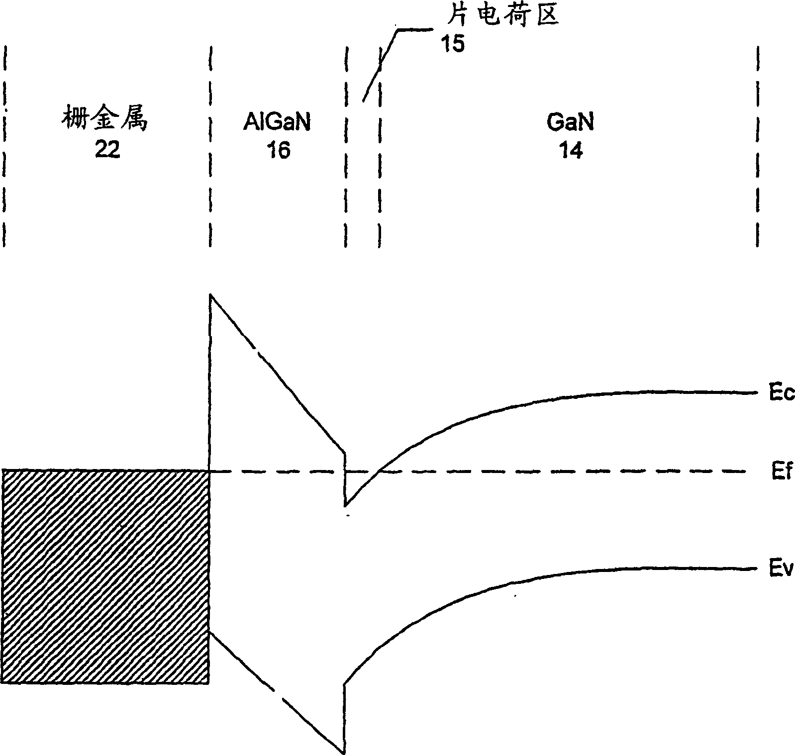
[0029] As mentioned above, it is well known tha...


PUM

PropertyMeasurementUnit
Thicknessaaaaaaaaaa
Thicknessaaaaaaaaaa

Abstract

High electron mobility transistors (HEMTs) and methods of fabricating HEMTs are provided. Devices according to embodiments of the present invention include a gallium nitride (GaN) channel layer and an aluminum gallium nitride (AlGaN) barrier layer on the channel layer. A first ohmic contact is provided on the barrier layer to provide a source electrode and a second ohmic contact is also provided on the barrier layer and is spaced apart from the source electrode to provide a drain electrode. A GaN-based cap segment is provided on the barrier layer between the source electrode and the drain electrode. The GaN-based cap segment has a first sidewall adjacent and spaced apart from the source electrode and may have a second sidewall adjacent and spaced apart from the drain electrode. A non-ohmic contact is provided on the GaN-based cap segment to provide a gate contact. The gate contact has a first sidewall which is substantially aligned with the first sidewall of the GaN-based cap segment. The gate contact extends only a portion of a distance between the first sidewall and the second sidewall of the GaN-based cap segment.

Description

[0001] related application [0002] This application is related to and claims U.S. Provisional Patent No. 60 / 250755, filed December 1, 2000, entitled "AlGaN / GaN HEMT with Improved Gate Barrier Layer and Low Access Resistance" Priority of the application, the disclosure of which is incorporated herein as if filed in its entirety. [0003] Statement of Government Interest [0004] This invention was developed at least in part under Contract No. N00014-99-C-0657 of the Naval Research Institute. Therefore, the government has certain rights in this patent. technical field [0005] The present invention relates to a high electron mobility transistor (HEMT), and more particularly to an aluminum gallium nitride (AlGaN) / gallium nitride (GaN) high electron mobility transistor (HEMT). Background technique [0006] AlGaN / GaN HEMT (High Electron Mobility Transistor) devices are well known in the semiconductor field. US Patents 5192987 and 5296395 describe AlGaN / GaN HEMT structures an...

Claims


Application Information

Patent Timeline
IPC IPC(8): H01L21/28H01L21/338H01L29/20H01L29/423H01L29/778H01L29/812
CPCH01L29/2003H01L29/42316H01L29/7783H01L29/778
Inventor R·P·史密斯
Owner CREE INC
Why Eureka
Try Eureka