Sputter source, sputtering device, and sputtering method

A sputtering device and sputtering source technology, applied in sputtering plating, ion implantation plating, coating, etc., can solve problems such as difficult large-scale substrate films, large deviations in film quality, etc.

Active Publication Date: 2005-02-02
ULVAC INC
View PDF2 Cites 26 Cited by
  • Summary
  • Abstract
  • Description
  • Claims
  • Application Information

AI Technical Summary

Problems solved by technology

Like this, with the sputtering source of prior art, the film quality deviation of the formed film is big, it is difficult to form the thin film of film quality uniform on the large substrate.

Method used


Image

  • Sputter source, sputtering device, and sputtering method
  • Sputter source, sputtering device, and sputtering method
  • Sputter source, sputtering device, and sputtering method

Examples


Embodiment Construction

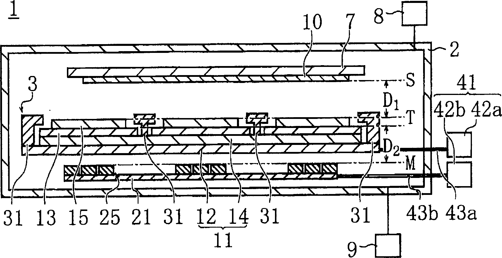
[0032] Embodiments of the present invention are described below with reference to the drawings. figure 1 Symbol 1 in represents a sputtering apparatus using the sputtering source of the present invention. This sputtering apparatus 1 has a vacuum chamber 2, a substrate holder 7 arranged on the ceiling side inside the vacuum chamber 2, and a sputtering source 3 arranged at a position opposite to the lower side of the substrate holder 7 inside the vacuum chamber 2. .

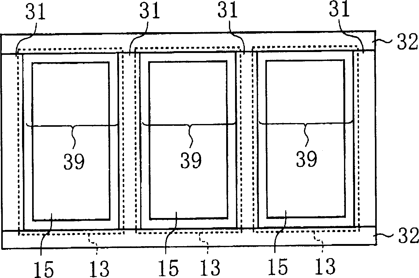
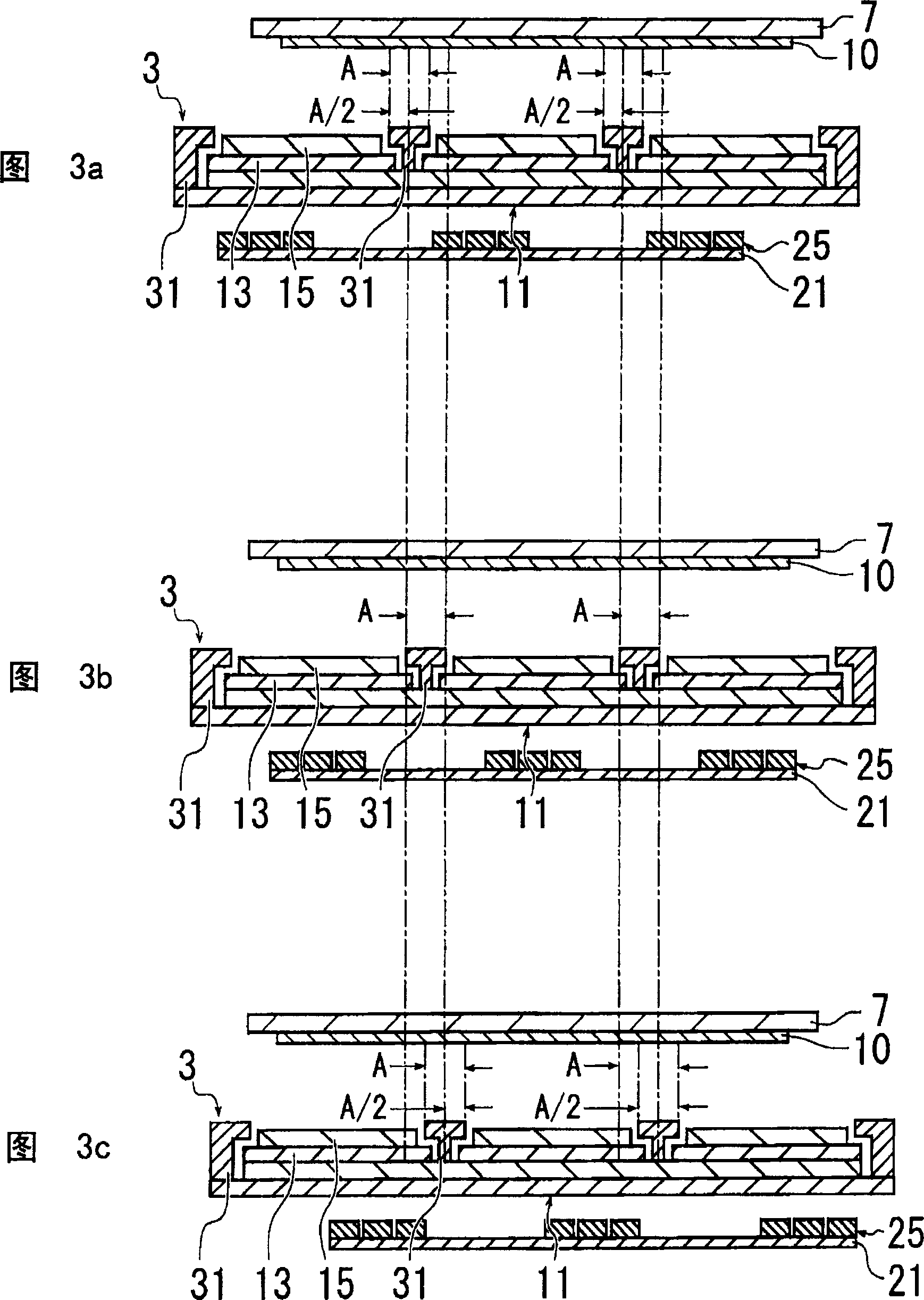
[0033] The sputtering source 3 has a target mounting plate 11 . A plurality of elongated anode electrodes 31 are separately arranged on the target mounting plate 11 in parallel with each other. like figure 2 As shown, elongated connection electrodes 32 are arranged at both ends of each anode electrode 31 . Each anode electrode 31 and connection electrodes 32 at both ends are connected to each other, and an opening 39 is formed through these electrodes 31 , 32 .

[0034] The cathode electrode 13 is arranged i...


PUM


Abstract

When sputtering a target 15, each target 15 is moved with respect to the substrate 10. Therefore, the entire area of the substrate 10 faces the target 15 at sputtering, which enables the formation of the film with a uniform quality on the surface of the substrate 10. At sputtering, not only the target 15 but also a magnetic field-forming unit 25 are moved with respect to the target 15, so a large area of the target 15 can be sputtered. If the magnetic field-forming unit 25 is moved with respect to the substrate 10, an extensively sputtered area of the target 15 is moved with respect to the substrate 10, which yields a more uniform quality distribution in the film formed on the substrate 10.

Description

technical field [0001] The invention relates to a magnetron sputtering device. Background technique [0002] In recent years, with the increase in the size of the substrate as the object of film formation, the sputtering source is also required to be increased in size, but it is difficult to increase the size of the target, such as Figure 6 As shown, a sputtering source 103 with a plurality of small targets 115 is therefore considered. The targets 115 of the sputtering source 103 are juxtaposed on the same plane, and the anode electrodes 113 are disposed between the targets 115 . [0003] The surface of each target 115 is opposed to the substrate as the object of film formation, and the magnetic field forming device 125 is respectively arranged on the back side, and the sputtering gas is introduced into the vacuum chamber in which the sputtering source 103 is placed, and each anode electrode 113 is placed at the ground potential. In a state where voltage is applied to each...

Claims


Application Information

Patent Timeline
Patent Type & Authority Applications(China)
IPC IPC(8): C23C14/34C23C14/08C23C14/35H01J37/34
CPCC23C14/086H01J37/3408H01J37/3455C23C14/352C23C14/34
Inventor 佐藤重光末代政辅大空弘树清田淳也中村肇石桥晓太田淳
Owner ULVAC INC
Why Eureka
Try Eureka