
Time delay computing method, timing analytic method, approximating method for calculating object network and delay control method

A calculation method, a technology of delay control, applied in computer-aided design, devices that perform calculation operations by changing electric quantity or magnetic quantity, calculation, etc.

Inactive Publication Date: 2005-02-09
PANASONIC CORP
View PDF1 Cites 2 Cited by
  • Summary
  • Abstract
  • Description
  • Claims
  • Application Information

AI Technical Summary

Problems solved by technology

[0010] However, due to the increase in the inter-wiring capacitance and the increase in the wiring resistance accompanying the miniaturization of processing, the power supply voltage for reducing power consumption is lowered, and as Figure 30 As shown, the signal migration changes the potential of the adjacent net, and the power supply or zero potential approximation of the adjacent net gradually becomes invalid.

Method used


Image

  • Time delay computing method, timing analytic method, approximating method for calculating object network and delay control method
  • Time delay computing method, timing analytic method, approximating method for calculating object network and delay control method
  • Time delay computing method, timing analytic method, approximating method for calculating object network and delay control method

Examples


Embodiment approach 1

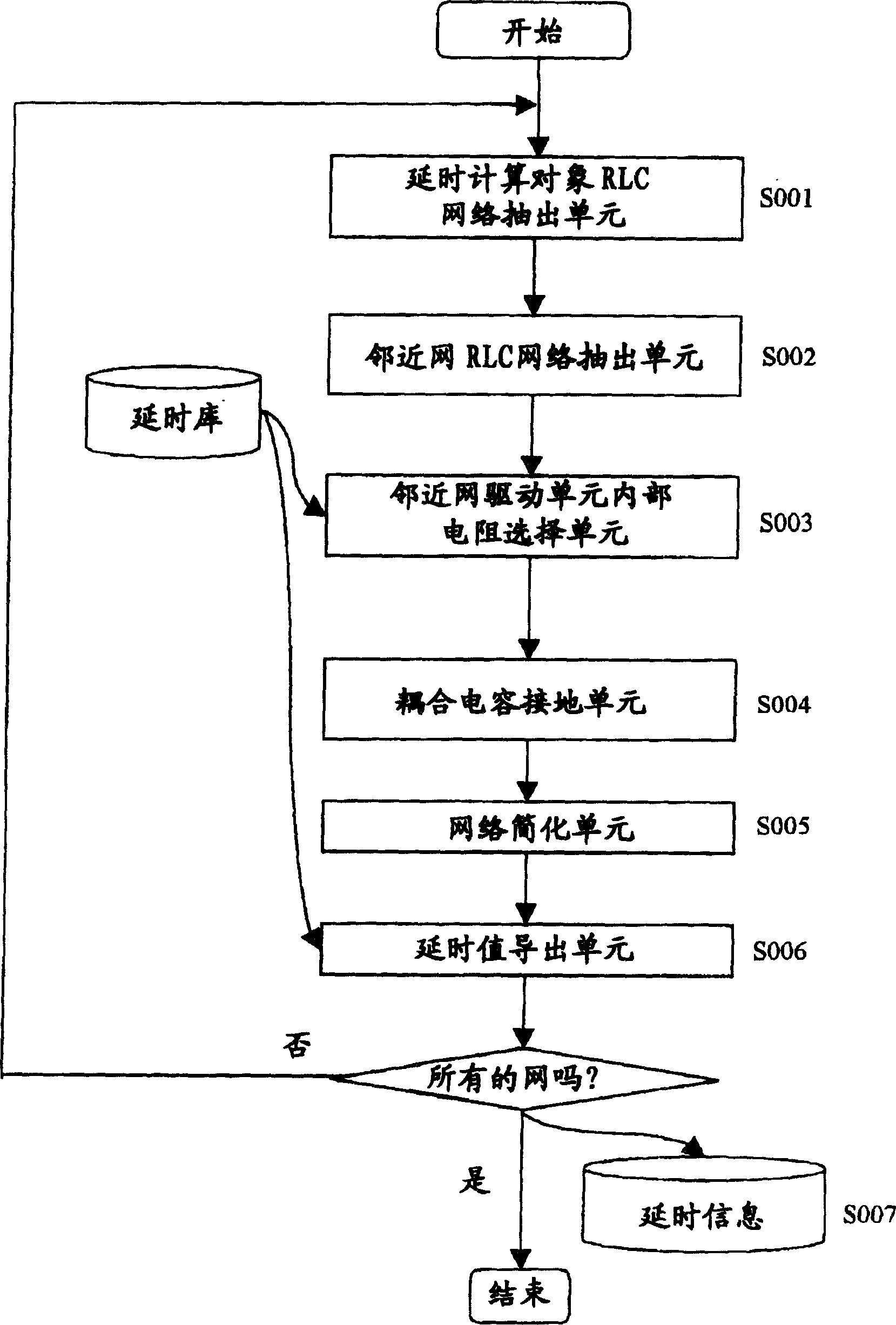
[0085] First, regarding the delay calculation method of the semiconductor integrated circuit design in Embodiment 1 of this invention, by Figure 1 to Figure 6 Be explained. Embodiment 1 is a delay calculation method that takes into account the influence on the delay value of delay calculation target nets based on adjacent delay calculation target nets during delay calculation.

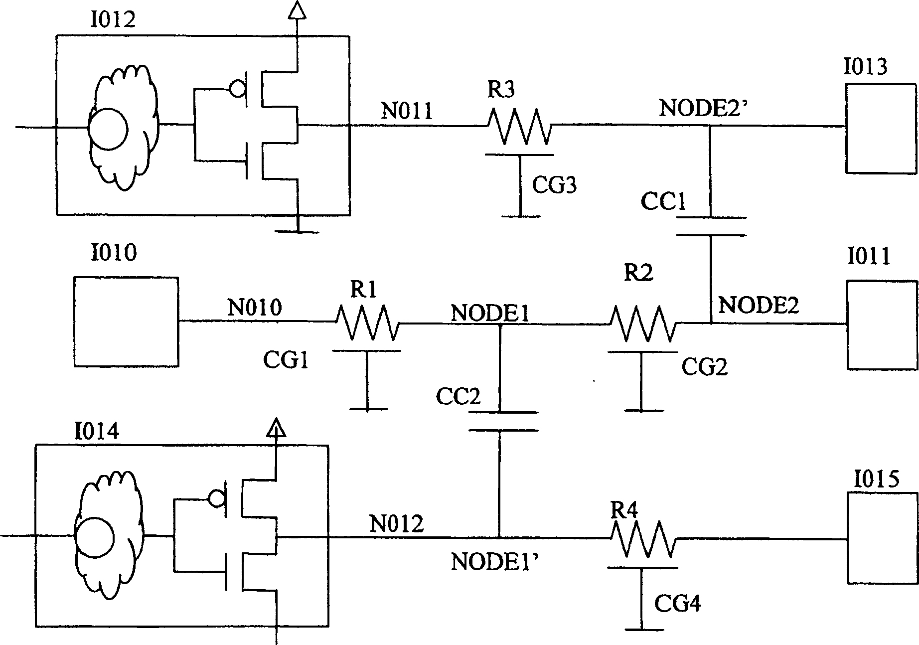
[0086] figure 1 It is a flowchart showing the procedure of the delay calculation method of Embodiment 1. figure 2It is a circuit diagram composed of net N010 composed of sample 1010 and sample 1011, net N011 composed of sample 1012 and sample 1013, and net N012 composed of sample 1014 and sample 1015. The net N010 is connected to the net N011 by the inter-wiring capacitance CC1 and the net N012 by the inter-wiring capacitance CC2. In addition, the wiring resistors R1 and R2 and the ground capacitance CG1 and CG2 are parasitic on the net N010, the line resistance R3 and the ground capacitance CG3 ...

Embodiment approach 2

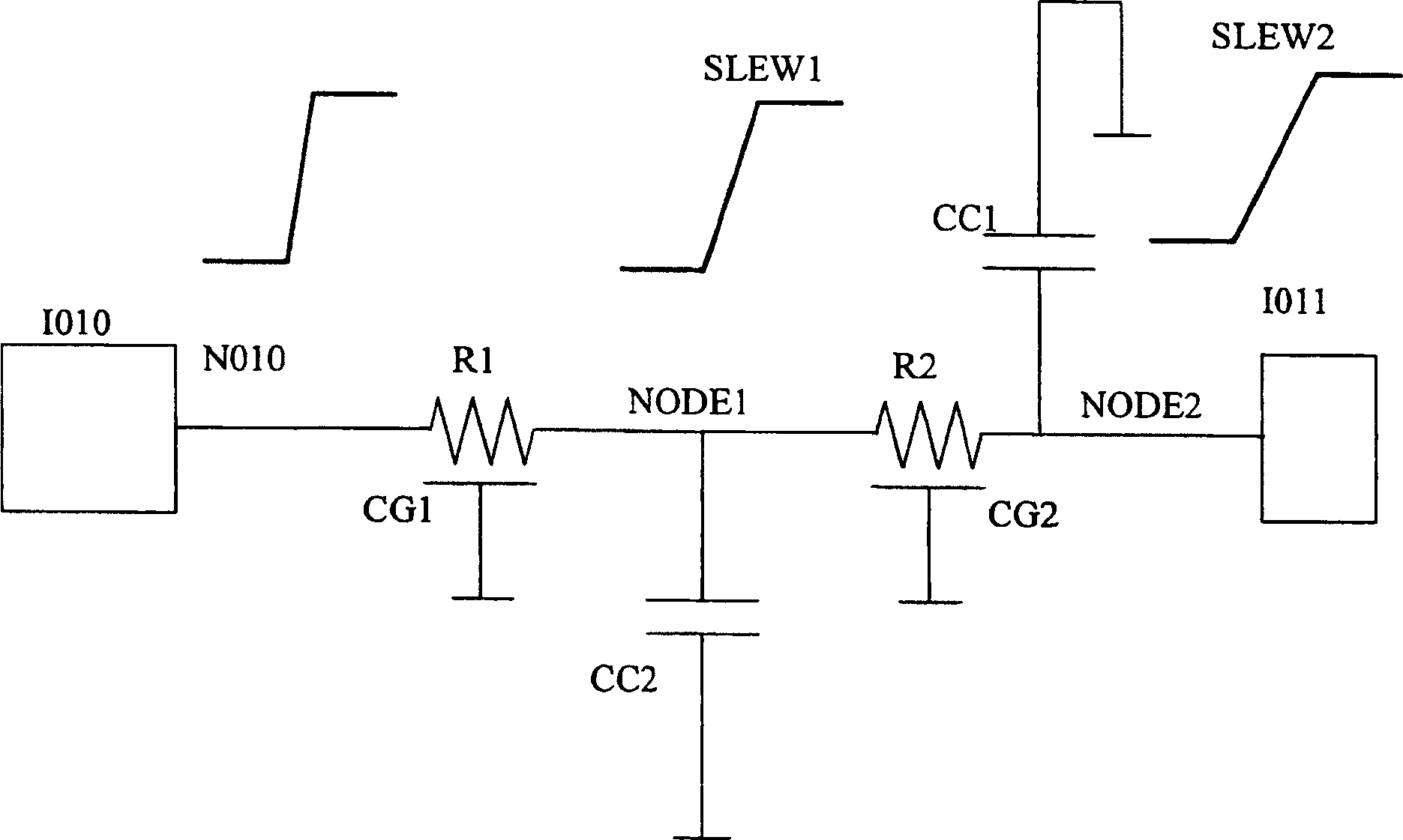
[0092] Regarding the delay calculation method of semiconductor integrated circuit design according to Embodiment 2 of this invention, by Figure 2 ~ Figure 4 , Figure 7 ~ Figure 9 illustrate. This second embodiment is a delay calculation method that considers the influence of the delay value of the delay calculation target net due to the net adjacent to the delay calculation target net during the delay calculation.

[0093] Figure 7 It is a flowchart showing the procedure of the delay calculation method of Embodiment 2. figure 2 It is a circuit diagram composed of net N010 composed of sample 1010 and sample 1011, net N011 composed of sample 1012 and sample 1013, and net N012 composed of sample 1014 and sample 1015. The net N010 is connected to the net N011 by the inter-wiring capacitance CC1 and the net N012 by the inter-wiring capacitance CC2. Furthermore, wiring resistors R1 and R2, ground capacitances CG1 and CG2 are on net N010, wire resistance R3 and ground capacit...

Embodiment approach 3

[0099] A timing analysis method for semiconductor integrated circuit design according to Embodiment 3 of the present invention, particularly a static timing analysis method, will be described.

[0100] This Embodiment 3 is a timing that performs strict analysis at regular intervals for setting and maintaining timing constraints in consideration of the influence on the delay value of a net in a timing analysis target route based on a net adjacent to a net in a timing analysis target route. parsing method.

[0101] Figure 10 It is a flowchart showing the procedure of the timing analysis method according to the third embodiment. Figure 11 is a net with net N020 from clock source CK to flip-flop FF1, net N023 from clock source CK to flip-flop FF2, combinatorial circuit COMB1 and net N021 as a path from flip-flop FF1 to flip-flop FF2, adjacent net N020 A synchronous sequential circuit of N024, net N025 adjacent to net N021, and net N026 adjacent to net N023.

[0102] Taking th...


PUM


Abstract

A delay calculation method considering a net adjacent to a delay calculation object net of a semiconductor integrated circuit includes: an adjacent net internal resistance selecting step of selecting a combination of static state of an adjacent net driving cell; a coupling capacitance grounding step of multiplying a coupling capacitance by a coefficient obtained from an internal resistance of the adjacent net driving cell selected by the adjacent net internal resistance selecting step, and the like, and grounding the value obtained thereby as the coupling capacitance of the delay calculating object net; and a delay value deriving step of deriving the delay value from a circuit obtained by these steps. A problem of the delay calculation method that an accurate delay value cannot be obtained because in actuality, the adjacent wire whose potential fluctuates is approximated to zero potential is solved by this structure.

Description

[0001] technology area [0002] The present invention relates to a delay calculation method, a timing analysis method, and a calculation target network for increasing the overall delay time in a fabricated semiconductor device or increasing the speed of arbitrary wiring, which are used in a CAD device for assisting in the design of a semiconductor device, etc. Approximation method and delay control method. Background technique [0003] In recent years, due to the miniaturization of semiconductor processing, the capacitance between adjacent wirings has increased compared with the capacitance to the substrate and the gate capacitance. Therefore, delay calculations using CAD devices that take the capacitance between wirings into account have become mainstream. In addition, a method of analyzing the potential variation time of adjacent wirings while maintaining the time range by the static analysis method, and calculating the delay variation due to the capacitance between adjacent...

Claims


Application Information

Patent Timeline
Patent Type & Authority Applications(China)
IPC IPC(8): G06F17/50G06G7/00H01L21/82H01L27/04H03K5/14
CPCG06F17/5036G06F30/367
Inventor 雨河直树一宫敬弘佐藤和弘
Owner PANASONIC CORP
Learn More