Method of forming narrow trenches in semiconductor substrates

A semiconductor and substrate technology, applied in the field of forming narrow trenches, can solve problems such as helping, and achieve the effect of reducing gate charges

Inactive Publication Date: 2005-03-09
GEN SEMICON
View PDF4 Cites 2 Cited by
  • Summary
  • Abstract
  • Description
  • Claims
  • Application Information

AI Technical Summary

Problems solved by technology

On the other hand, the oxide film at the bottom of the trench does not significantly contribute to channel formation, but still contributes to the gate charge

Method used


Image

  • Method of forming narrow trenches in semiconductor substrates
  • Method of forming narrow trenches in semiconductor substrates
  • Method of forming narrow trenches in semiconductor substrates

Examples


Embodiment Construction

[0022] The present invention is described more fully hereinafter with reference to the accompanying drawings, in which preferred embodiments of the invention are shown. This invention may, however, be embodied in various forms and should not be construed as limited to the embodiments set forth herein.

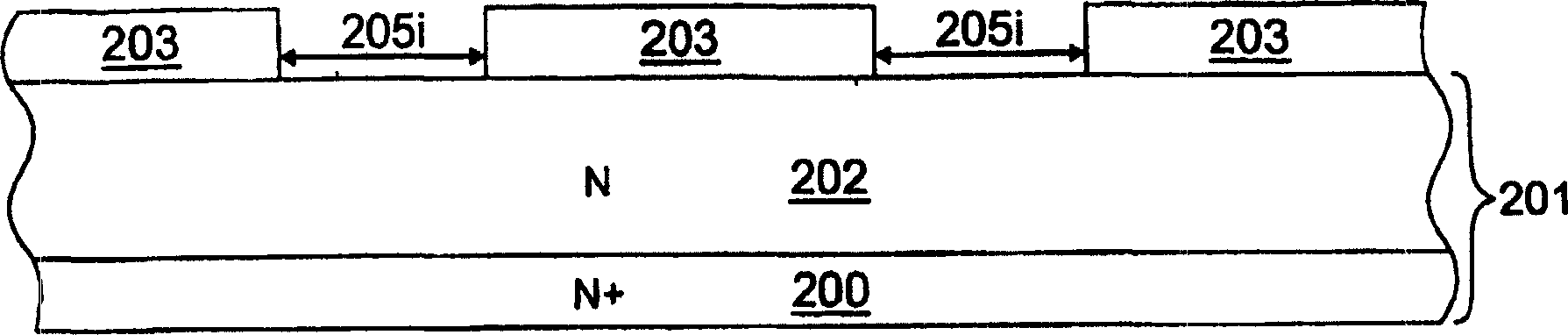
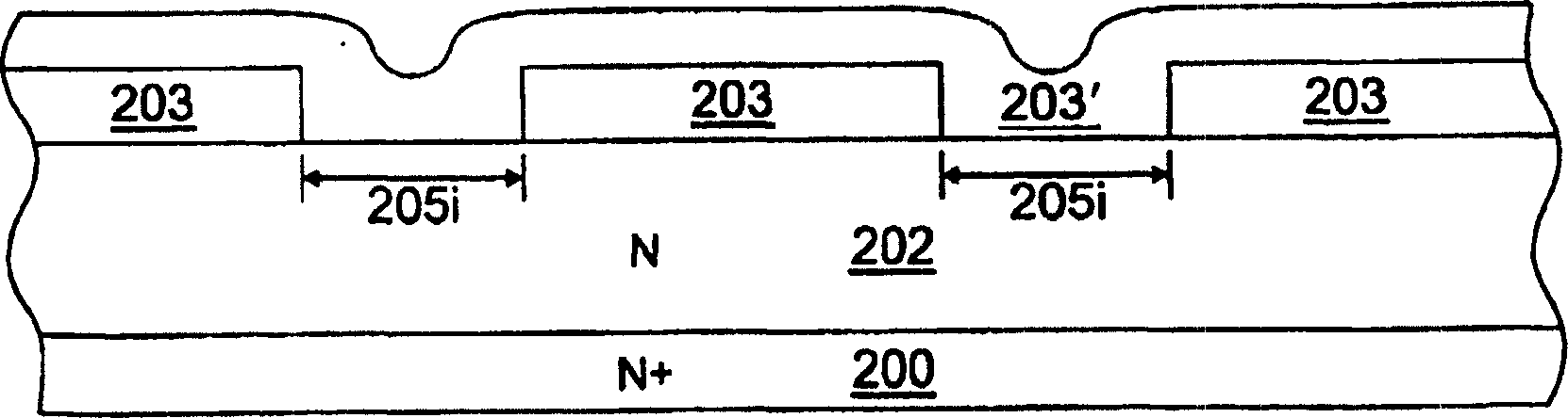
[0023] According to an embodiment of the present invention, a semiconductor substrate is a preferred substrate. The semiconductor substrate may be any substrate in the known technology, including elemental semiconductor substrates such as silicon or germanium, or compound semiconductor substrates such as GaAs, AlAs, GaP, InP, GaAlAs and the like. A semiconductor substrate can be monocrystalline, polycrystalline and / or amorphous, and it can be doped or undoped. according to Figures 2A to 2D Specific examples of semiconductor substrates are presented. refer to Figure 2A , shows a silicon semiconductor substrate 201 consisting of an N+ doped silicon wafer 200 having an N dope...


PUM


Abstract

A method of forming a trench (207) within a semiconductor substrate (202) by providing a patterned first CVD-deposited masking material layer (203) having a first aperture over the semiconductor substrate (202). A second masking layer material is CVD-deposited and etched to form spacers (203s) in the first aperture, the spacers (203s) form a second aperture narrower than the first aperture. The semiconductor substrate (202) is etched through the second aperture such that a trench (207) is formed in the semiconductor substrate (202). In preferred embodiments, the method of the present invention is used in the formation of trench MOSFET devices.

Description

technical field [0001] The present invention relates to methods of forming narrow trenches in semiconductor substrates. Background technique [0002] Narrow trenches are often desired in the fabrication of wide arrays of semiconductor devices. Thus, while specific examples of the utility of narrow trenches are discussed below in connection with trench MOSFET devices, it should be noted that narrow trenches have utility throughout the semiconductor field. [0003] A trench MOSFET (Metal-Oxide Semiconductor Field Effect Transistor) is a transistor in which a channel is formed vertically and a gate is formed in a trench extending between source and drain regions. A trench lined with a thin insulating layer, such as an oxide layer, and filled with a conductor, such as polysilicon (ie, polycrystalline silicon), allows less compressive current flow and thus provides lower specific on-resistance values. Examples of trench MOSFET transistors are disclosed, for example, in US Paten...

Claims


Application Information

Patent Timeline
Patent Type & Authority Applications(China)
IPC IPC(8): H01L21/28H01L21/3065H01L21/308H01L21/336H01L21/8234H01L27/088H01L29/12H01L29/423H01L29/49H01L29/78
CPCH01L21/3088H01L21/3086H01L21/18
Inventor 石甫渊苏根政约翰·E·阿马托布赖恩·D·普拉特
Owner GEN SEMICON
Why Eureka
Try Eureka