Trench MOSFET with trenched floating gates having thick trench bottom oxide as termination

a technology of trench bottom oxide and floating gate, which is applied in the direction of semiconductor devices, electrical devices, transistors, etc., can solve the problems of limiting the shrinkage of the device cell, the inability to meet the requirements of the device, so as to achieve the effect of improving performan

Active Publication Date: 2013-09-03
FORCE MOS TECH CO LTD
View PDF3 Cites 3 Cited by
  • Summary
  • Abstract
  • Description
  • Claims
  • Application Information

AI Technical Summary

Benefits of technology

[0008]It is therefore an object of the present invention to provide a new and improved semiconductor power device such as a trench MOSFET with better performance than prior art by offering a semiconductor power device comprising: a plurality of first type trenched gates filled with conductive material padded by a gate insulating layer in active area, extending from top surface of a silicon layer of a first conductivity type, surrounded by source regions of the first conductivity type encompassed in body regions of a second conductivity type near the top surface; and the gate insulating layer comprising a composite bottom oxide on bottom of each first type trenched gates, comprising a thick bottom oxide and a pad oxide beneath, wherein the thick bottom oxide having greater thickness than sidewall oxide along sidewalls of each first type trenched gates. In some preferred embodiment, the thick oxide can be implemented by high density plasma (HDP) oxide. Therefore, the interface state gate charge between the trench bottom and the HDP oxide is reduced because of the inducing of the pad oxide.
[0009]It is another object of the present invention to further apply trenched source-body contact filled with metal plug between every adjacent of the first type trenched gates for achieving cell size shrinkage and eliminating the trade-off between the Sbs and the HDP oxide thickness discussed above. In some preferred embodiment, the trenched source-body contact can be implemented by forming vertical sidewalls or slope sidewalk penetrating through a contact insulating layer lying over the silicon layer, further through the source regions and extending into the body regions.
[0011]It is another object of the present invention to further apply multiple of third type trenched gates as trenched floating gates in termination area having thick trench bottom oxide and body region extending between adjacent of said third type trenched gates to further enhance breakdown voltage.
[0013]It is another object of the present invention to further apply a manufacturing method with three masks process, therefore, no additional parasitic bipolar transistor is built in near the second type trenched gate in gate contact area, thus enhancing the avalanche capability.

Problems solved by technology

However, the trench MOSFET 100 and the manufacturing method of prior art still encounter difficulties and limitations for device shrinkage and gate charge reduction.
Second, planar source-body contact is used in the trench MOSFET 100 of prior art, limiting device cell shrinkage as the planar source-body contact occupying large space and causing poor contact performance.
Furthermore, a trade-off between a space Sbs (the space defining P body and n+ source regions, as illustrated in FIG. 1) and thickness of the HDP oxide 115 causes a difficulty in optimization of device performance because the both are determined by wet etching time for removal of trenched gates sidewall oxide in manufacturing processes.
The longer Sbs, the thinner the HDP 115 resulting in higher Qgd; the shorter Sbs, the less n+ source regions formed into the P body regions resulting in less contact area to source metal 160, leading to high contact resistance and poor contact performance.
Meanwhile, near the trenched gate in gate contact area, which is positioned between the termination area and the active area, additional parasitic bipolar transistor with floating n+ source regions is built, causing poor avalanche capability because the parasitic bipolar transistor is easily turned on.

Method used


Image

  • Trench MOSFET with trenched floating gates having thick trench bottom oxide as termination
  • Trench MOSFET with trenched floating gates having thick trench bottom oxide as termination
  • Trench MOSFET with trenched floating gates having thick trench bottom oxide as termination

Examples


Embodiment Construction

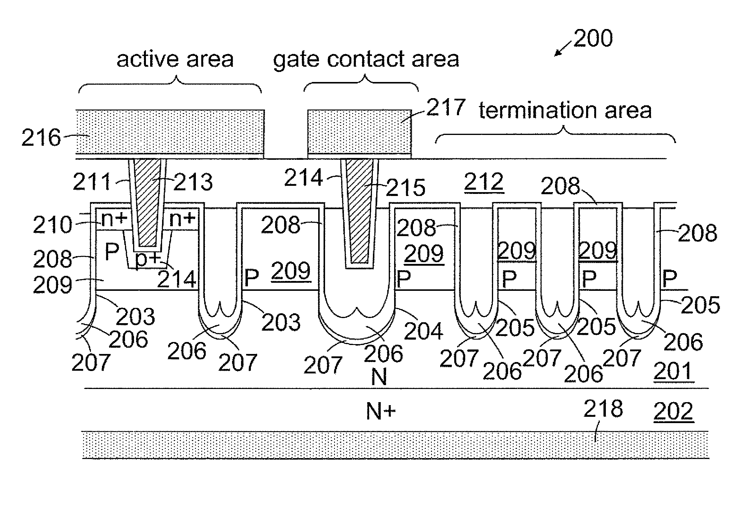
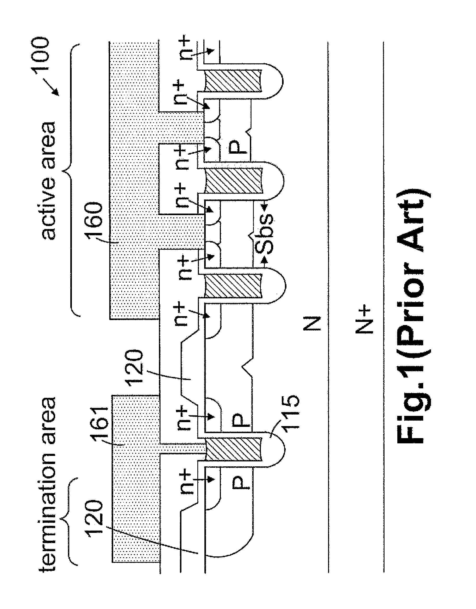
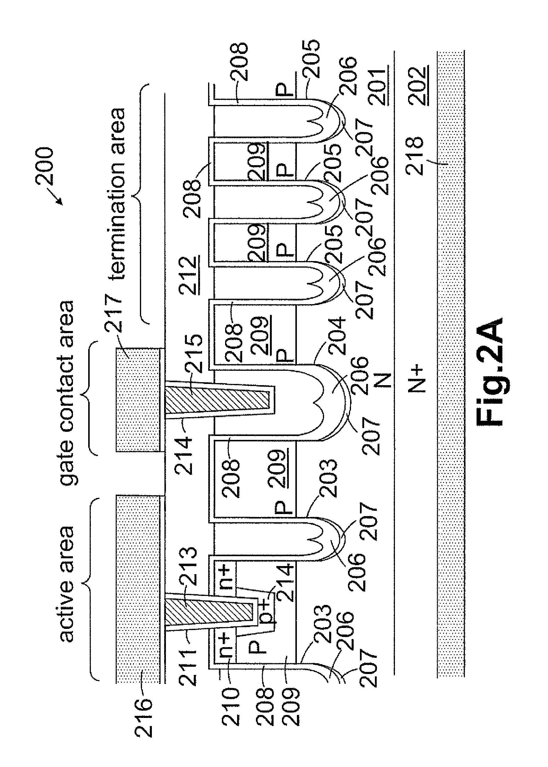
[0029]Please refer to FIG. 2A for a preferred N-channel trench MOSFET 220 with composite oxide as trench bottom oxide for reduced gate charge according to the present invention. The N-channel trench MOSFET 200 is formed in an N epitaxial layer 201 supported on a heavily doped N+ substrate 202 which coated with back metal 218 on the rear side as drain electrode, in some preferred embodiment, the N+ substrate 202 can be implemented by using a red phosphorus substrate. A plurality of trenched gates are formed extending from top surface of the N epitaxial layer 201, among those trenched gates, including: a plurality of first type trenched gates 203 in active area, at least one second type trenched gate 204 in gate contact area and multiple of third type trenched gates 205 in termination area. Some preferred embodiment includes following features: the second type trenched gates 204 has greater trench width than the first type trenched gates 203; the third type trenched gates 205 have gre...


PUM


Abstract

A power semiconductor power device having composite trench bottom oxide and multiple trench floating gates is disclosed. The gate charge is reduced by forming a pad oxide surrounding a HDP oxide on trench bottom. The multiple trenched floating gates are applied in termination for saving body mask.

Description

[0001]This application is a continuation in part of U.S. patent application Ser. No. 12 / 591,467 filed on Nov. 20, 2009.FIELD OF THE INVENTION[0002]This invention relates generally to the cell structure, device configuration and fabricating method of semiconductor power devices. More particularly, this invention relates to configuration and fabricating method of an improved trench MOSFET (Metal Oxide Semiconductor Field Effect Transistor) having thick trench bottom oxide and multiple trenched floating gates in termination area.BACKGROUND OF THE INVENTION[0003]In field of semiconductor power devices, it is desirable to further reduce Qgd (charge between gate and drain) for less power consumptions and higher switching speed, for a trench MOSFET (Metal Oxide Semiconductor Field Effect Transistor), such purposes are generally achieved by implementing a thick trench bottom oxide in trenched gates of the trench MOSFET. Meanwhile, it is also desirable to simplify the manufacturing processes...

Claims


Application Information

Patent Timeline
Patent Type & Authority Patents(United States)
IPC IPC(8): H01L29/78
CPCH01L29/66825H01L27/11521H01L27/11531H01L29/66621H01L29/407H01L29/4236H01L29/66727H01L29/66734H01L29/7811H01L29/7813H01L27/11519H01L29/1095H01L29/41766H01L29/456H01L29/0619H01L29/086H01L29/0869H01L29/0878H10B41/10H10B41/30H10B41/42
Inventor HSIEH, FU-YUAN
Owner FORCE MOS TECH CO LTD
Why Eureka
Try Eureka