Laterally diffused metal oxide semiconductor structure and method for forming same

A technology of oxide semiconductors and conductors, applied in semiconductor devices, semiconductor/solid-state device manufacturing, electrical components, etc., can solve the problem of large gate charge Qgd, limited high-frequency application of semiconductor structures, and inability to maintain high-voltage breakdown resistance of structures Performance and other issues, to achieve the effect of reducing gate charge and high breakdown voltage

Pending Publication Date: 2018-10-19
SILERGY SEMICON TECH (HANGZHOU) CO LTD
View PDF5 Cites 2 Cited by
  • Summary
  • Abstract
  • Description
  • Claims
  • Application Information

AI Technical Summary

Problems solved by technology

Therefore, when the semiconductor structure 100 is in the off state, the potential on the thick oxygen layer Oxdie cannot assist in depleting the N-type drift region N-drift, and the high voltage breakdown resistance of the structure cannot be maintained.
In addition, the gate electrode extends to the top of the N-type drift region N-drift, and the gate-drain region overlap is relatively large, so that the gate charge Qgd is relatively large, which limits the high-frequency application of the semiconductor structure 100

Method used


Image

  • Laterally diffused metal oxide semiconductor structure and method for forming same
  • Laterally diffused metal oxide semiconductor structure and method for forming same
  • Laterally diffused metal oxide semiconductor structure and method for forming same

Examples


Embodiment Construction

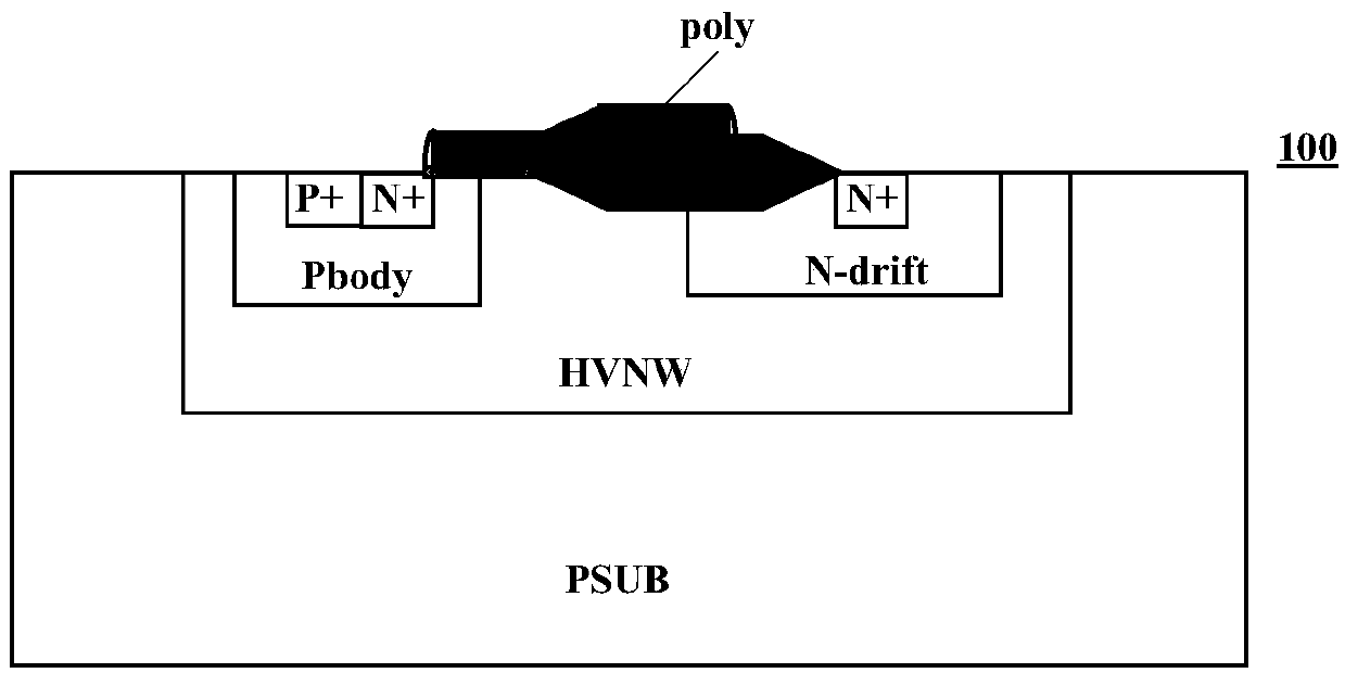
[0066] Hereinafter, the present invention will be described in more detail with reference to the accompanying drawings. In the various drawings, the same components are denoted by similar reference numerals. For the sake of clarity, various parts in the drawings have not been drawn to scale. Also, some well-known parts may not be shown. For simplicity, the structure obtained after several steps can be described in one figure. In the following, many specific details of the present invention are described, such as the structure, material, size, process and technique of each constituent part, for a clearer understanding of the present invention. However, the invention may be practiced without these specific details, as will be understood by those skilled in the art.

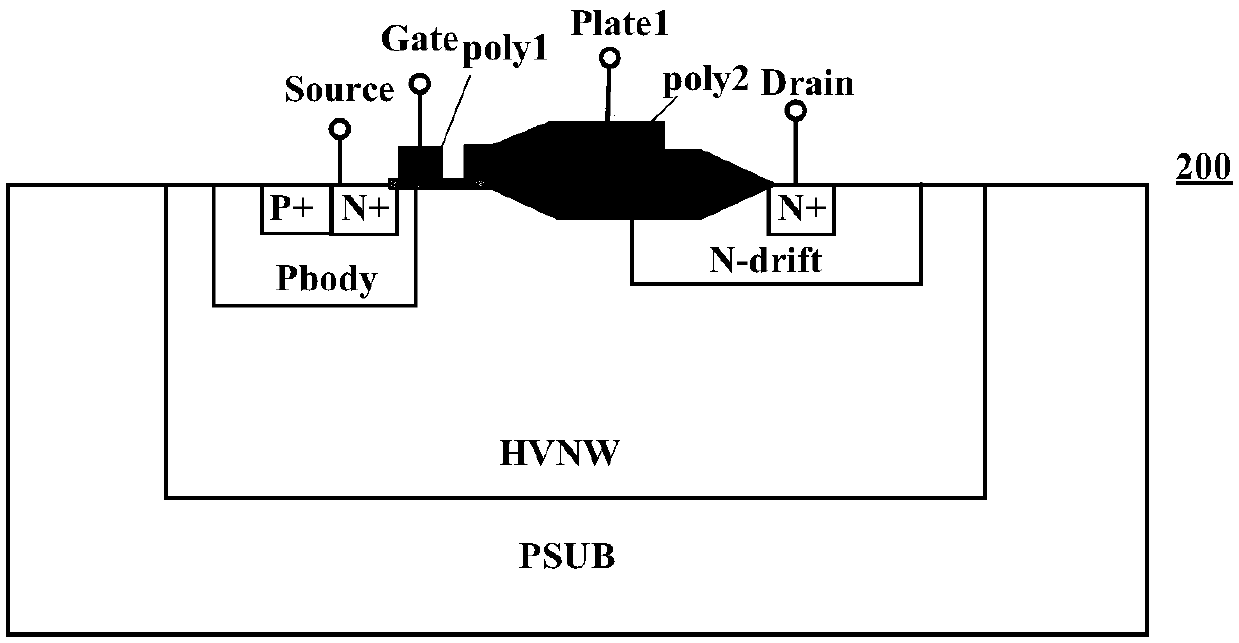
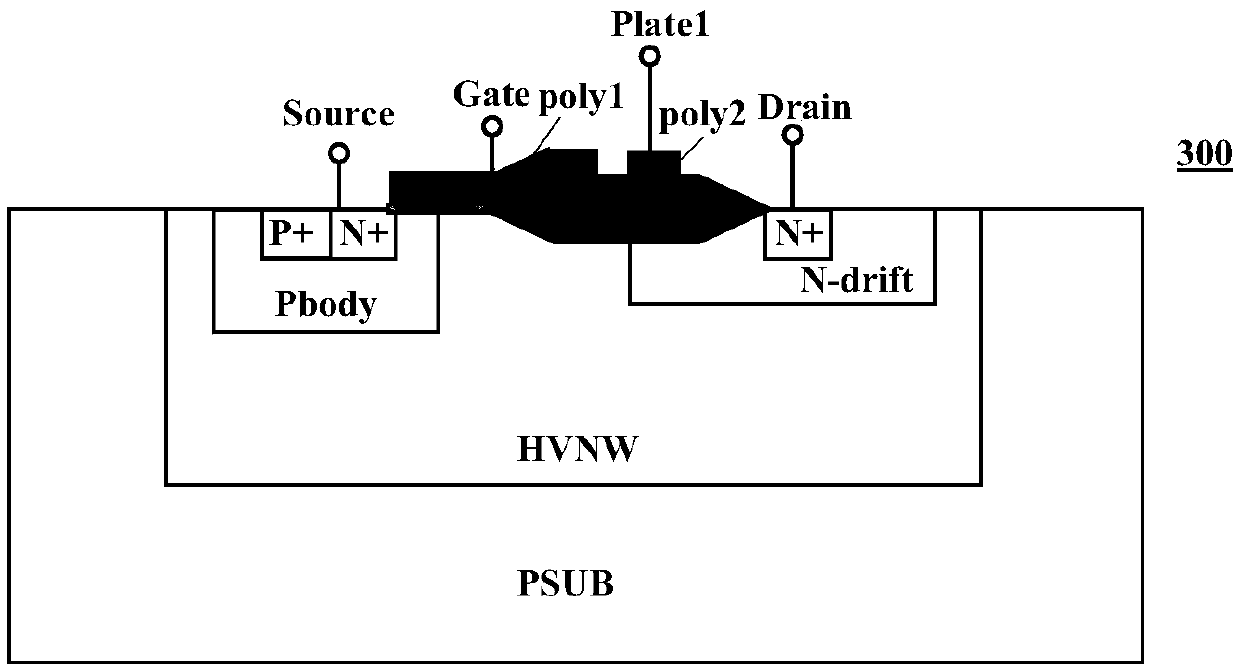
[0067] figure 2 It is a schematic structural diagram of a laterally diffused metal oxide semiconductor structure 200 according to Embodiment 1 of the present invention. The semiconductor structure provided acc...


PUM


Abstract

The present invention provides a laterally diffused metal oxide semiconductor structure and a method for forming the same. A conductor layer located above a first dielectric layer and a voltage-withstanding layer is divided into a first conductor which is at least partially located in the first dielectric layer and a second conductor which is at least partially located on the voltage-withstandinglayer, thus the first conductor and the second conductor are spatially isolated and can be connected to different potentials such that the semiconductor structure maintains a high breakdown voltage ina shutdown state. Furthermore, an interface between the first dielectric layer and the voltage-withstanding layer is covered by one of the first conductor and the second conductor, the gate charge ofthe semiconductor structure can be effectively reduced, and so that the semiconductor structure is adapted to high frequency applications.

Description

technical field [0001] The present invention relates to the technical field of semiconductors, and more particularly, to a laterally diffused metal oxide semiconductor structure and a forming method thereof. Background technique [0002] In the existing laterally diffused metal oxide semiconductor structure 100 such as figure 1 As shown, it generally includes a P-type substrate PSUB, a high-voltage N-type well region HVNW located in the P-type substrate PSUB, and a P-type body region Pbody and an N-type drift region N-drift are formed in the high-voltage N-type well region HVNW , the source region N+ and the drain region N+ are respectively formed in the P-type body region Pbody and the N-type drift region N-drift, and the body contact region P+ is also formed in the body region Pbody and is in contact with the source region N+, and in The surface of the semiconductor structure 100 is also provided with a gate dielectric layer (not marked in the figure) adjacent to the sour...

Claims


Application Information

Patent Timeline
Patent Type & Authority Applications(China)
IPC IPC(8): H01L29/78H01L29/06H01L21/336
CPCH01L29/0688H01L29/66409H01L29/78H01L29/063H01L29/1095H01L29/402H01L29/7816H01L29/24H01L29/42368H01L29/404H01L29/405H01L29/66681H01L29/66704
Inventor 游步东喻慧王猛杜益成彭川黄贤国
Owner SILERGY SEMICON TECH (HANGZHOU) CO LTD
Why Eureka
Try Eureka