Quick switch IGBT structure

A fast switching and gate structure technology, applied in the direction of electrical components, circuits, semiconductor devices, etc., can solve the problems of gate overshoot voltage, large Miller capacitance of devices, and affecting turn-on characteristics, so as to reduce capacitance and improve transient Effect of switching speed and gate charge reduction

Active Publication Date: 2019-05-28
江苏矽导集成科技有限公司
View PDF8 Cites 3 Cited by
  • Summary
  • Abstract
  • Description
  • Claims
  • Application Information

AI Technical Summary

Problems solved by technology

[0004] However, the conductance modulation effect occurs in the N-drift region 4 when the IGBT of this structure is turned on, and a large number of carriers are stored, resulting in a relatively slow turn-off process of the device.
In addition, the device Miller capacitance (gate collector capacitance) is large, which affects the turn-on characteristics, causes gate overshoot voltage, and restricts device performance

Method used


Image

  • Quick switch IGBT structure
  • Quick switch IGBT structure
  • Quick switch IGBT structure

Examples


Embodiment Construction

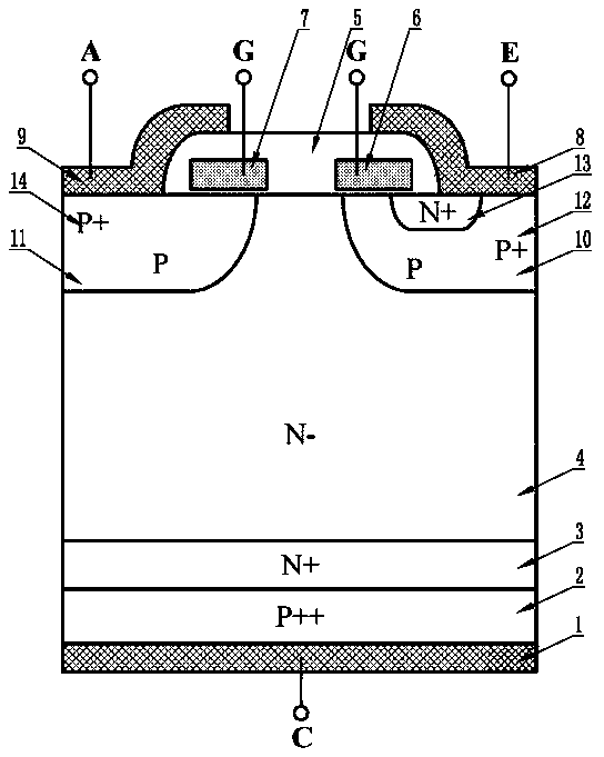
[0021] Such as figure 2 The fast switching IGBT structure shown includes a collector 1, a P++ collector region 2, an N+ buffer region 3, an N-drift region 4, a gate structure and a top metal layer stacked sequentially from bottom to top. Wherein, the gate structure includes a gate dielectric layer 5 , a first gate electrode 6 and a second gate electrode 7 . In this embodiment, the gate structure adopts a planar structure, the gate dielectric layer 5 is disposed on the top of the N-drift region 4 , and the first gate electrode 6 and the second gate electrode 7 are arranged horizontally and separately on the gate dielectric layer 5 . The top metal layer includes an emitter 8 and an auxiliary electrode 9 arranged separately.

[0022] Such as figure 2 As shown, a first P-type base region 10 and a second P-type base region 11 are separately arranged on the upper part of the N-drift region 4 . A first P+ emitter region 12 and an N+ emitter region 13 are arranged on the top of t...


PUM


Abstract

The invention discloses a quick switch IGBT structure comprising a collector, a P++ collector region, an N+ buffer region, an N-drift region, a gate structure and a top metal layer which are laminatedfrom bottom to top, wherein the gate structure comprises a gate dielectric layer, a first gate electrode and a second gate electrode, the top metal layer comprises an emitter and an auxiliary electrode, a first P-type base region and a second P-type base region are arranged at the upper part of the N-drift region, a first P+ emitter region and an N+ emitter region are arranged at the upper part of the first P-type base region, the first P+ emitter region and the N+ emitter region are connected with the emitter, the first P-type base region and the N+ emitter region correspond to the first gate electrode, a second P+ emitter region is arranged at the upper part of the second P-type base region, the second P + emitter region is connected with the auxiliary electrode, the second P-type baseregion corresponds to the second gate electrode or the first gate electrode, an inductor L1 is connected between the auxiliary electrode and the emitter, an inductor L2 is connected between the emitter and an external terminal, and the inductor L1 and the inductor L2 form mutual inductance. The structure can greatly improve the transient switching speed of the device.

Description

technical field [0001] The invention relates to the technical field of power semiconductor devices, in particular to an insulated gate bipolar transistor (IGBT). Background technique [0002] Insulated gate bipolar transistor (IGBT) is a new type of power electronic device combining MOS field effect and bipolar transistor. It not only has the advantages of easy driving and simple control of MOSFET, but also has the advantages of low conduction voltage of power transistor, large on-state current and low loss, so it is widely used in energy conversion, locomotive traction, industrial frequency conversion, automotive electronics and consumer electronics, etc. It is one of the important core devices in the field of power electronics. [0003] State-of-the-art IGBT structures such as figure 1 As shown, it includes collector electrode 1', P++ collector region 2', N+ buffer region 3', N-drift region 4', gate structure and emitter 5' stacked in sequence from bottom to top, wherein...

Claims


Application Information

Patent Timeline
Patent Type & Authority Applications(China)
IPC IPC(8): H01L29/739H01L29/423
Inventor 孙茂友宋李梅周丽哲
Owner 江苏矽导集成科技有限公司
Why Eureka
Try Eureka