Structure and fabrication process of super junction MOSFET

a technology of metal oxidesemiconductor and fabrication process, which is applied in the direction of basic electric elements, electrical apparatus, and semiconductor devices

Inactive Publication Date: 2013-12-10
WUXI VERSINE SEMICON CORP
View PDF6 Cites 2 Cited by
  • Summary
  • Abstract
  • Description
  • Claims
  • Application Information

AI Technical Summary

Benefits of technology

[0057]A vertical structure was used in the super junction MOSFET. A side-wall isolation structure was introduced underneath the source (or emitter) electrode. The same type of buffer area as the body area can be installed below the body area. The source electrode can also be extended downward at the external side of the side wall isolation structure to form a field plate. Due to the introduction of such buffer area and the field plate, the doping concentration in the drifting area can be much higher to effectively reduce the drain to source resistance Rdson and improve the FOM. Compared to conventional VDMOS which forms trenches at two sides of the integral gates, the actual gate coverage area can be made much smaller according to this invention. Thus the gate charge Qg can be reduced by reducing the gate coverage area. In addition, the actual comparative area of the gate and the electrode (drain electrode) below the substrate is smaller in comparison with the conventional VDMOS, which effectively reduces the gate drain charge Qgd. Furthermore, this invention has simpler fabrication process. The self alignment technology was used. Masks are only used for gate contact formation. Therefore, only three mask layers are needed for the whole process which is very cost effective.

Problems solved by technology

Its input impedance is high and driving power is small.
The manufacture of this traditional structure is rather complex.
Therefore, the production cost is relatively higher.

Method used


Image

  • Structure and fabrication process of super junction MOSFET
  • Structure and fabrication process of super junction MOSFET
  • Structure and fabrication process of super junction MOSFET

Examples


example 1

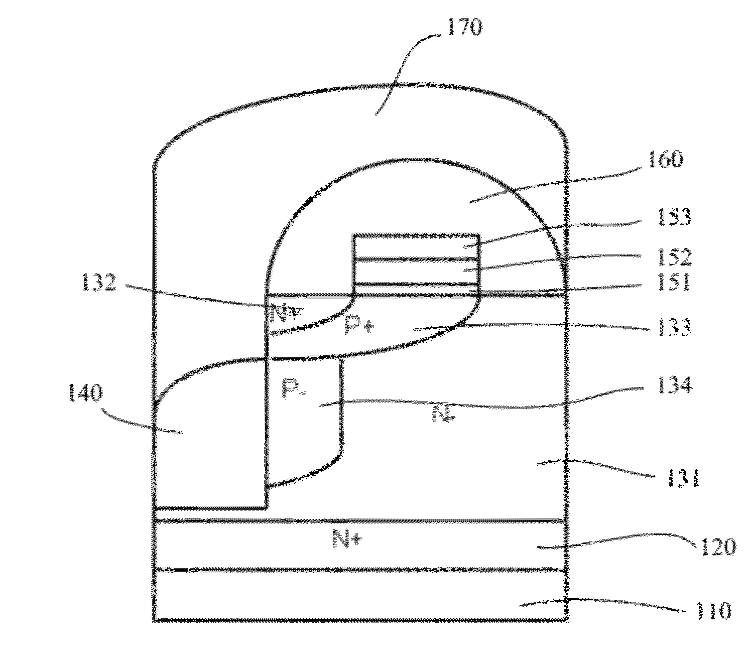
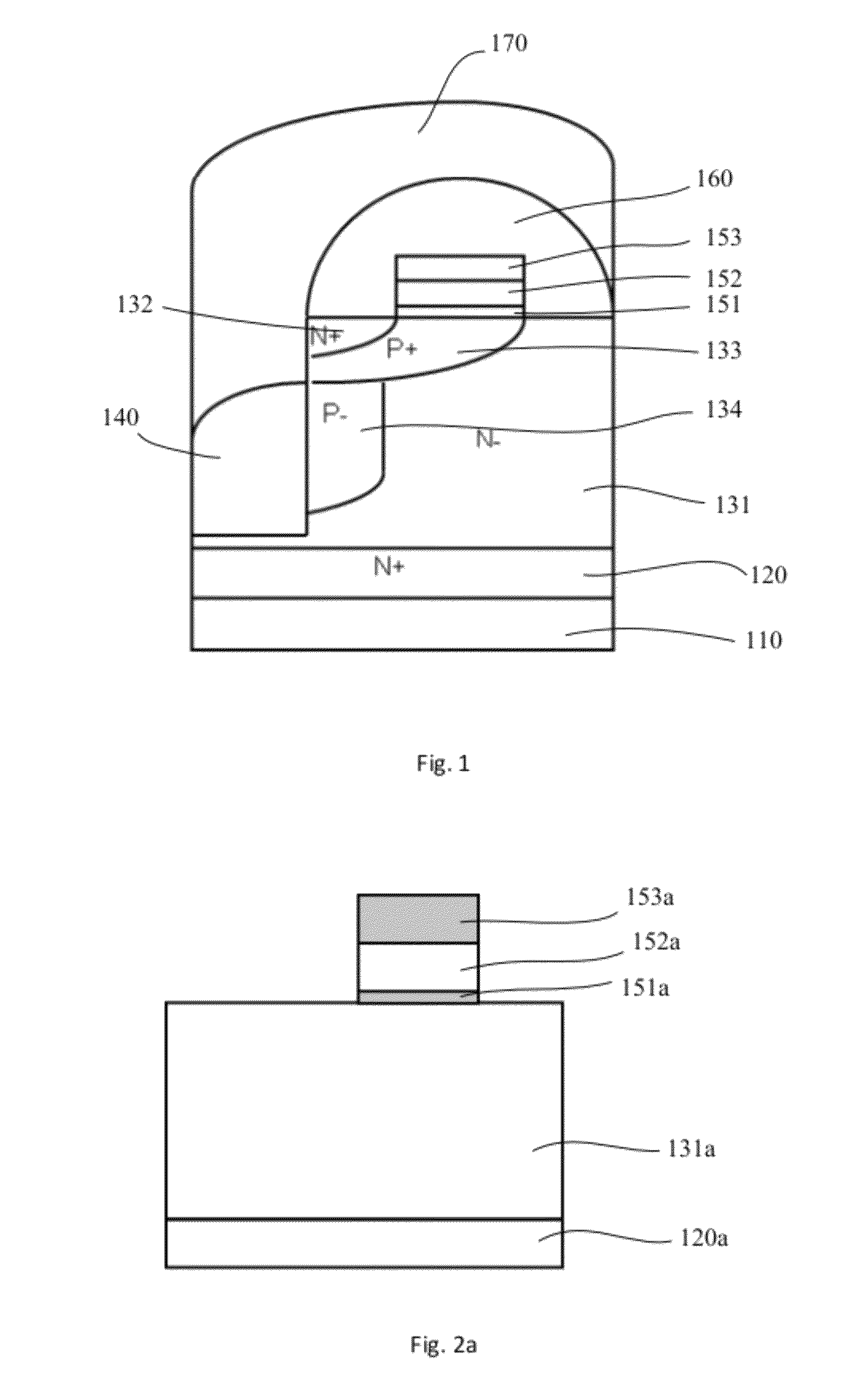
[0064]This example shows a MOSFET structure illustrated in FIG. 1. This device includes: a drain 110, the first conductive substrate 120, an active area, a side-wall isolation structure 140, a gate, a surface isolation structure 160 and a source 170.

[0065]The first conductive substrate 120 is above the drain 100. The active area is above the first conductive substrate 120. The active area includes the first conductive drift region 131, the first conductive source 132 above the first conductive drift region 131 and the first conductive source 132 and the second conductive body 133 between the first conductive source 132 and the first conductive drift region 131; the side-wall isolation structure 140 is above the first conductive substrate 120 and it contacts to the side-wall of said active area which is close to the first conductive source 132. The height of the side-wall isolation structure is lower than the active area such that the side-wall of the first conductive source 132 and ...

example 2

[0082]This example presents another super junction MOSFET device structure. As illustrated in FIG. 3, such device structure includes: a drain 210, the first conductive substrate 220, an active area, a side wall isolation structure 240, a gate, a surface isolation structure 260 and a source 270.

[0083]From bottom to top, the active area includes the first conductive drift region 231, the first conductive source 232 above 231, and the second conductive body between the first conductive source 232 and first conductive drift region 231. Inside the active area there is a second conductive buffer layer 234 which is underneath the second conductive body 233. It contacts with the second conductive body area 233, the side wall isolation structure 240 and the first conductive drift area 231. The second conductive buffer layer 234 is a second type lightly doped semiconductor material while the second conductive body 233 is a second type heavily doped semiconductor material. The gate includes a ...

example 3

[0085]This example presents another super junction power MOSFET device structure. As illustrated in FIG. 4, such structure includes: a drain 310, the first conductive substrate 320, an active area, a side wall isolation structure 340, a gate, a surface isolation structure 360 and a source 370.

[0086]From bottom to top, the active area includes the first conductive drift region 331, the first conductive source 332 above 331 and the second conductive body 333 between the first conductive source 332& first conductive drift area 331. The gate includes a gate dielectric 351 layer and a gate electrode 352 above it. There is an isolation layer 353 above the gate electrode 352. The source 370 includes the extended field plate along one side of the side wall isolation structure 340.

[0087]The difference from Example 2 is that such structure has no second conductive buffer layer. With the source field plate, the EPI doping can be higher even without the second conductive buffer layer so that to...


PUM


Abstract

This invention discloses a specific superjunction MOSFET structure and its fabrication process. Such structure includes: a drain, a substrate, an EPI, a source, a side-wall isolation structure, a gate, a gate isolation layer and source. There is an isolation layer inside the active area underneath the source. Along the side-wall of this isolation layer, a buffer layer with same doping type as body can be introduced & source can be extended down too to form field plate. Such buffer layer & field plate can make the EPI doping much higher than convention device which results in lower Rdson, better performance, shorter gate so that to reduce both gate charge Qg and gate-to-drain charge Qgd. The process to make such structure is simpler and more cost effective.

Description

[0001]The present application claims the priority of Chinese Application No. 201110089219.X filed Apr. 8, 2011, under 35 U.S.C. §119, which is hereby incorporated by reference.TECHNICAL FIELD[0002]The present invention discloses a structure and fabrication process for a super junction metal-oxide-semiconductor field-effect transistor (MOSFET), especially a MOSFET and an insulated gate bipolar transistor (IGBT) which belongs to the field of semiconductor device and its fabrication.BACKGROUND OF THE INVENTION[0003]VDMOS (vertical diffused power MOSFET) and IGBT are two most commonly used power transistors nowadays. IGBT is composed of BJT (bipolar junction transistor) and MOS, which has the advantage of high input impedance of MOSFET and low conduction voltage drop of BJT. It is a very suitable candidate to be used in areas such as AC electric motor, frequency converter, power switch, lighting circuit, traction and driving. VDMOS is a voltage control device. Under the proper control o...

Claims


Application Information

Patent Timeline
Patent Type & Authority Patents(United States)
IPC IPC(8): H01L29/78
CPCH01L29/0634H01L29/0653H01L29/407H01L29/41766H01L29/66727H01L29/7802H01L29/6634H01L29/7396H01L21/26586H01L29/1095
Inventor HUANG, QINBAI, YUMINGGAO, YANG
Owner WUXI VERSINE SEMICON CORP
Why Eureka
Try Eureka