Low-noise amplifier
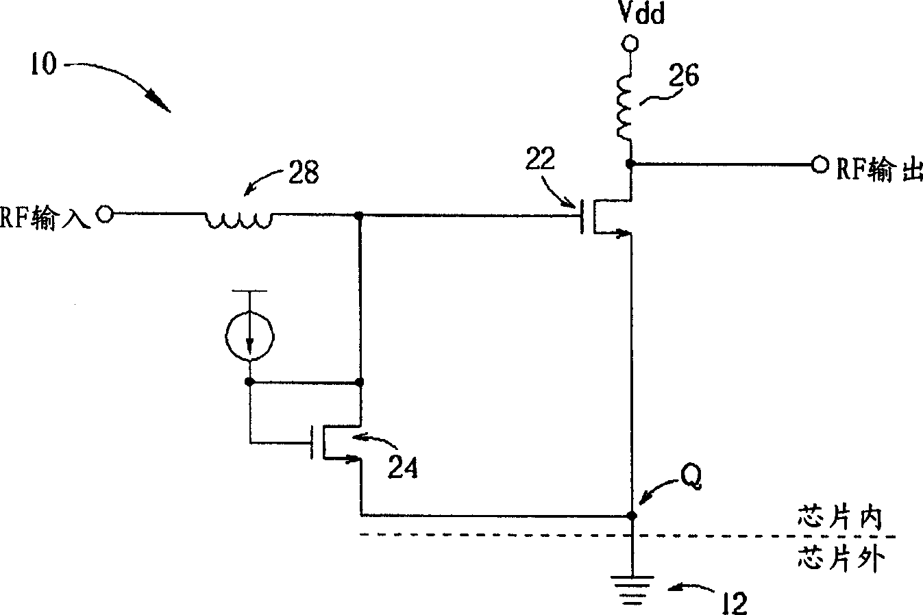
A low-noise amplifier and inductor technology, applied to amplifiers with only semiconductor devices, improved amplifiers to reduce noise effects, etc., can solve the problems of transistor 22 drain voltage instability, noise increase, power loss, etc., to achieve stable work range, large bandwidth, noise reduction effect
- Summary
- Abstract
- Description
- Claims
- Application Information
AI Technical Summary
Problems solved by technology
Method used
Image

Examples
Embodiment Construction
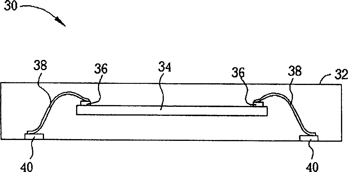
[0033] figure 2 is a schematic diagram of a chip 30 . The chip 30 includes a packaging structure 32 configured to protect a chip die 34 . Chip die 34 is electrically connected to an external connection point 40 of chip 30 through connection point 36 and wire bond 38 . Chip die 34 includes a low noise amplifier of the present invention. Accordingly, chip 30 may be mounted on a printed circuit board (PCB) or the like.
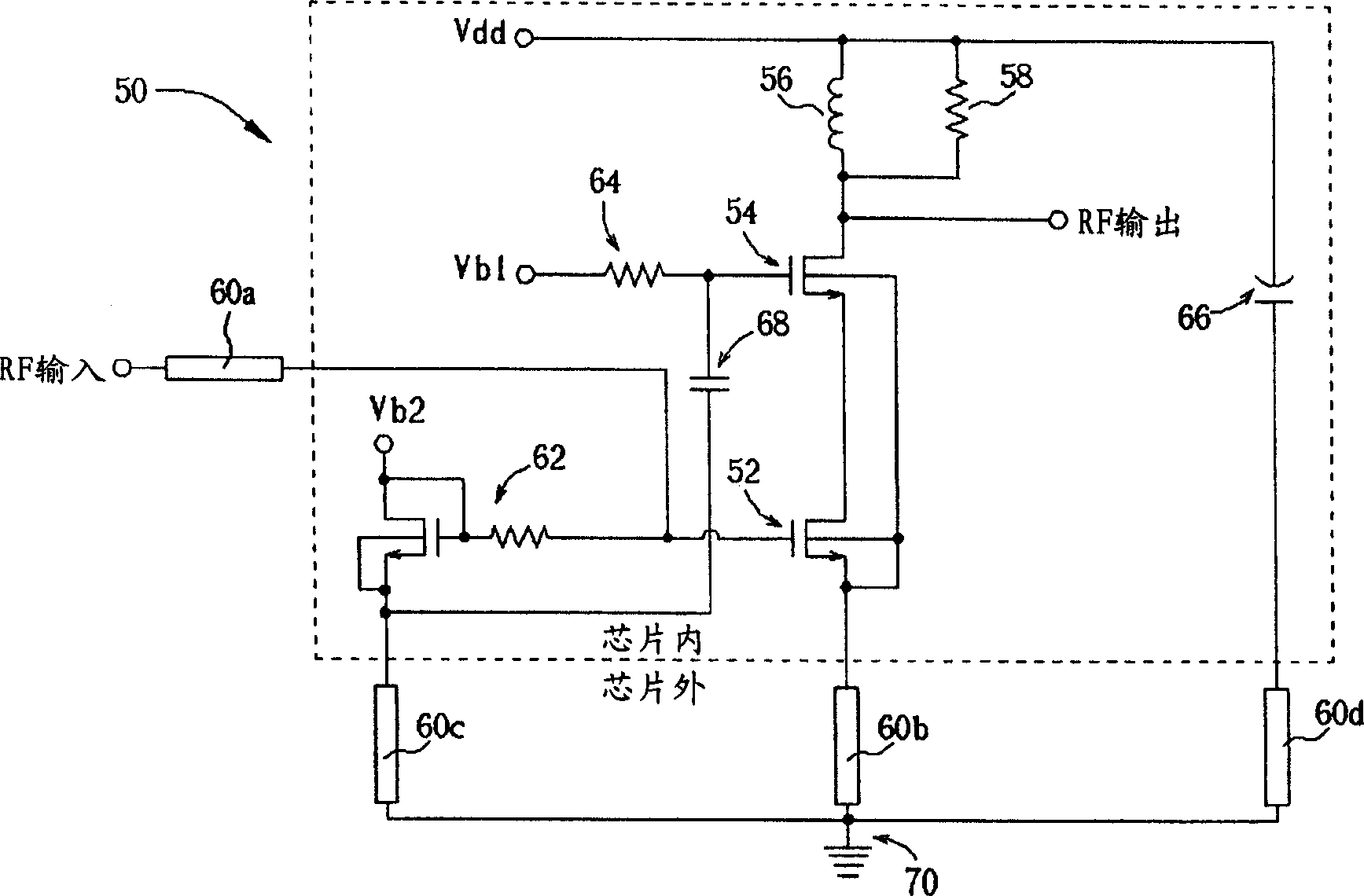
[0034] image 3 It is a schematic circuit diagram of a low noise amplifier 50 of the present invention, in image 3 The inside and outside of the chip are separated by a dotted line. The low noise amplifier 50 includes first and second transistors 52 , 54 , an inductor 56 and a first resistor 58 . The drain of the first transistor 52 is connected to the source of the second transistor 54 . The gate of the first transistor 52 is connected to an RF input node, and the source of the first transistor 52 is connected to an off-chip ground 70 . The gate of the...
PUM
 Abstract
Description
Claims
Application Information
 - R&D Engineer
- R&D Manager
- IP Professional
- Industry Leading Data Capabilities
- Powerful AI technology
- Patent DNA Extraction
Browse by: Latest US Patents, China's latest patents, Technical Efficacy Thesaurus, Application Domain, Technology Topic.
© 2024 PatSnap. All rights reserved.Legal|Privacy policy|Modern Slavery Act Transparency Statement|Sitemap