
Power-up circuit semiconductor memory device

A memory and semiconductor technology, applied in the field of power-on circuits of semiconductor memory devices, can solve problems such as threshold voltage reduction, unstable operation of semiconductor memory devices, abnormal power-on signal pwrup and early reset

Inactive Publication Date: 2005-07-13
SK HYNIX INC
View PDF0 Cites 3 Cited by
  • Summary
  • Abstract
  • Description
  • Claims
  • Application Information

AI Technical Summary

Problems solved by technology

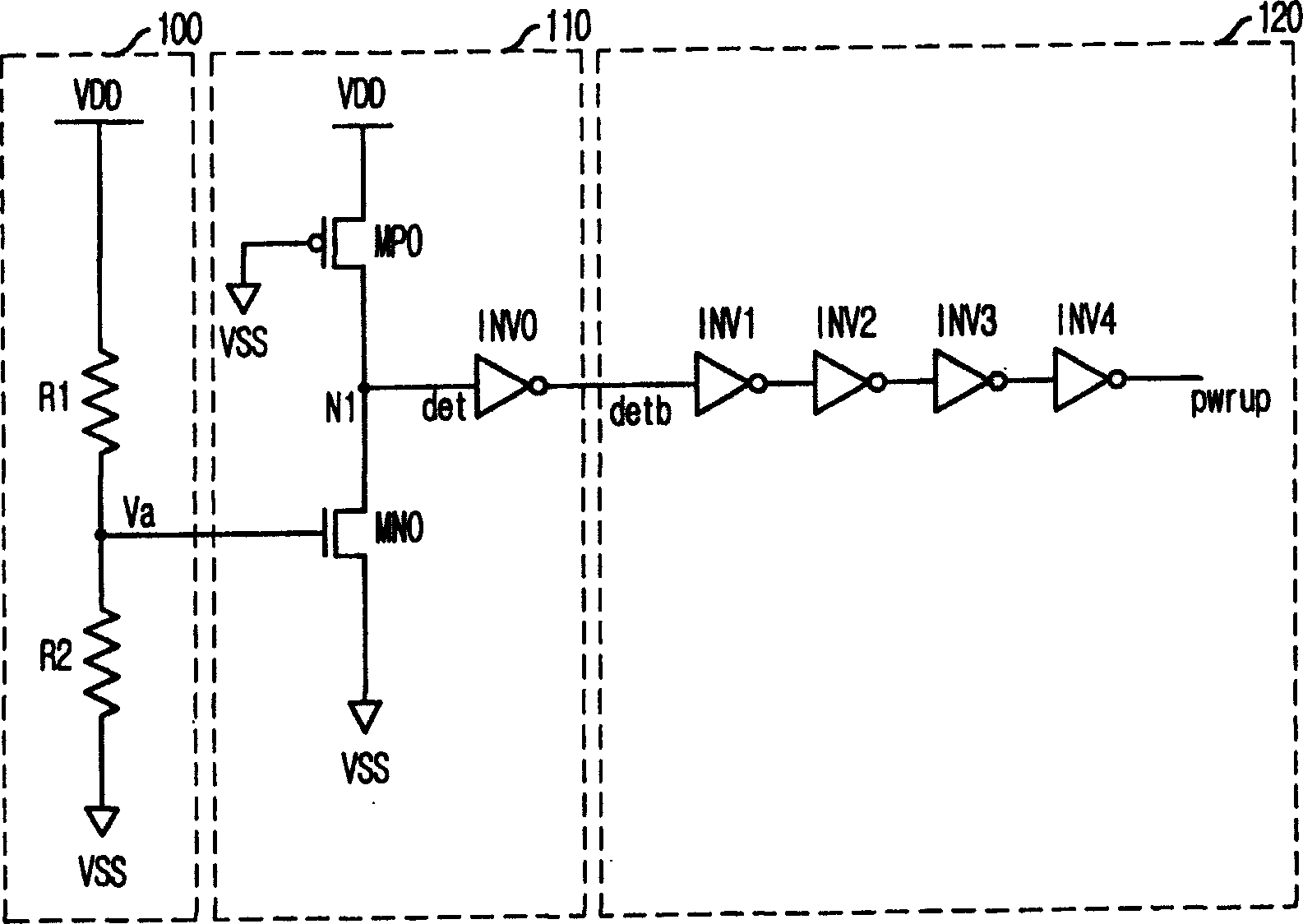
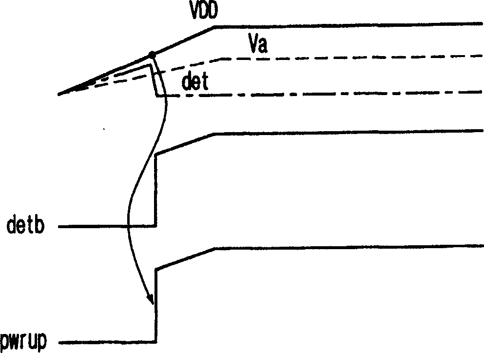
Therefore, if the MOS transistor becomes unstable due to some variation in the process, its threshold voltage will be lowered, causing the power-on signal pwrup to reset abnormally early
As a result, the abnormal early reset can lead to unstable operation of a semiconductor memory device

Method used


Image

  • Power-up circuit semiconductor memory device
  • Power-up circuit semiconductor memory device
  • Power-up circuit semiconductor memory device

Examples


Embodiment Construction

[0029] Hereinafter, a power-on circuit according to the present invention will be described in detail with reference to the accompanying drawings.

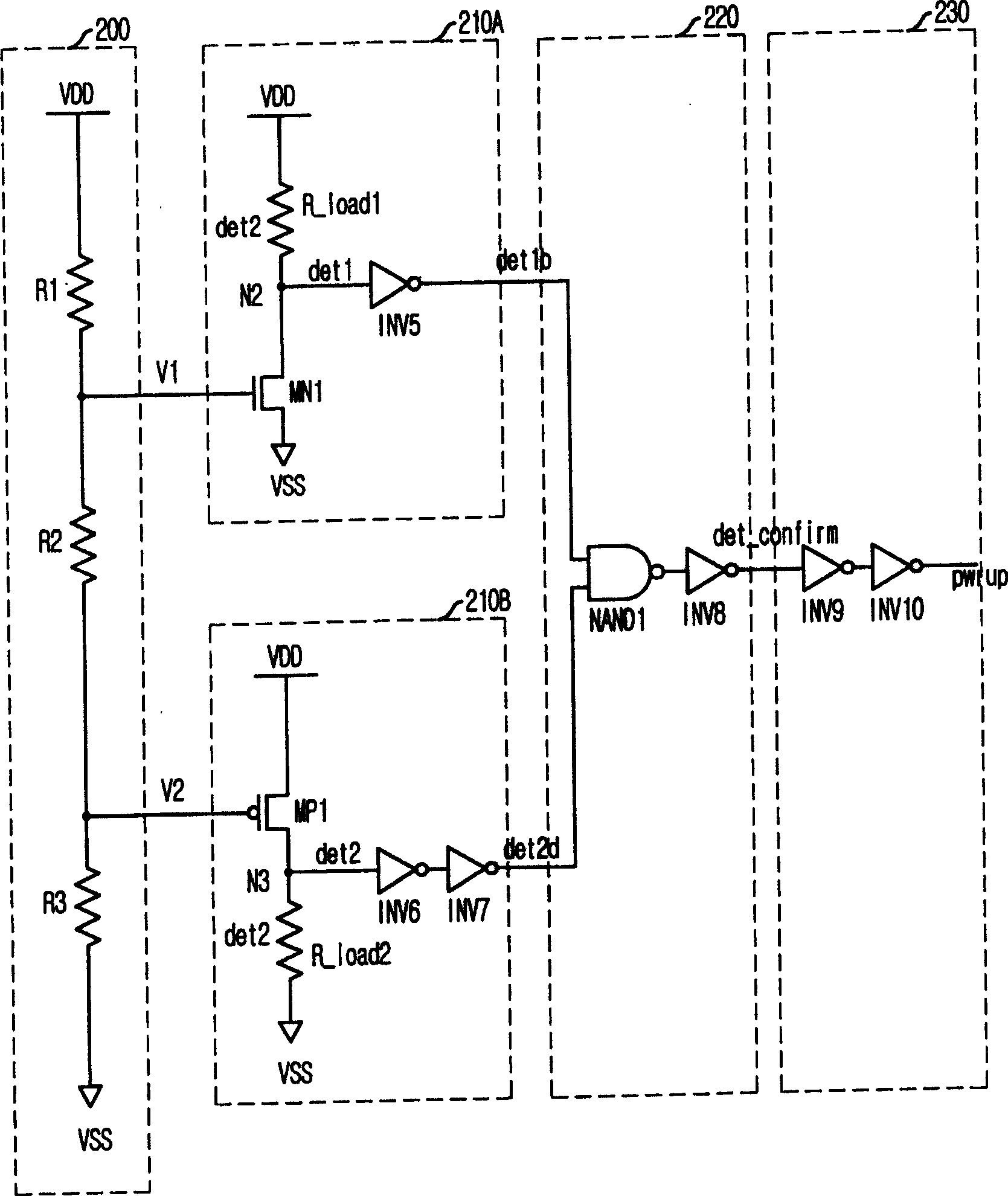
[0030] Fig. 3 is a schematic circuit diagram illustrating a power-up circuit according to a first preferred embodiment of the present invention.

[0031] As shown in the figure, the power-on circuit includes a power voltage level follower unit 200 , a first power voltage detection unit 210A, a second power voltage detection unit 210B, a summing unit 220 and a buffer unit 230 .

[0032] The supply voltage level follower unit 200 generates a first bias voltage V1 and a second bias voltage V2 which linearly increase or decrease in proportion to a voltage level of a supply voltage VDD.

[0033] The first power supply voltage detection unit 210A is used to detect that in response to the first bias voltage V1, the voltage level of the power supply voltage VDD will change to a threshold voltage corresponding to the threshold voltage of t...


PUM


Abstract

The power-on circuit includes a power supply voltage level follower unit for outputting a first bias voltage and a second bias voltage, which increase or decrease in proportion to a power supply voltage; the first power supply voltage detection unit is used for detecting: In response to the first bias voltage, the power supply voltage becomes a first threshold voltage level of the power supply voltage corresponding to the threshold voltage of the NMOS transistor; the second power supply voltage detection unit is used to detect: in response to the second bias voltage, the power supply voltage becoming a second threshold voltage level of the power supply voltage corresponding to the threshold voltage of the PMOS transistor; and a summation unit for performing a first detection signal output from the first power supply voltage detection unit and an output from the second power supply voltage A logic operation of the second detection signal of the detection unit, thereby outputting a confirmation signal, wherein the confirmation signal is activated when the power supply voltage satisfies both the first and second threshold voltage levels.

Description

technical field [0001] The present invention relates to a semiconductor device; and more particularly to a power-up circuit for a semiconductor memory device. Background technique [0002] In a semiconductor memory device, various internal logic and internal voltage generating blocks are provided for stabilizing operations of elements included in the semiconductor memory device. Before the semiconductor memory device is normally operated, the internal logic should be initialized to a predetermined state. [0003] The internal voltage generating block provides a bias voltage to the internal logic. After supplying a power supply voltage VDD, if the internal voltage does not reach an appropriate voltage level, some problems such as a latch-up phenomenon that degrades the reliability of the semiconductor memory device may occur. Therefore, a semiconductor memory device is provided with a power-on circuit for initializing the internal logic and preventing a latch-up phenomenon ...

Claims


Application Information

Patent Timeline
Patent Type & Authority Applications(China)
IPC IPC(8): G11C7/00G11C7/20G11C11/4072H03K17/22H03L7/00
CPCH03K17/223G11C7/00
Inventor 都昌镐李在真
Owner SK HYNIX INC
Learn More