Light emitting device and manufacturing method thereof

A technology of light-emitting devices and grooves, which is applied in the direction of semiconductor devices, electrical components, and the structure of active regions, and can solve problems such as the limitation of the light-emitting area of ​​the active layer

Inactive Publication Date: 2005-07-13
LG ELECTRONICS INC
View PDF0 Cites 15 Cited by
  • Summary
  • Abstract
  • Description
  • Claims
  • Application Information

AI Technical Summary

Problems solved by technology

[0014] However, in this conventional light-emitting device, since the buffer layer, n-contact layer, and active layer are sequentiall

Method used


Image

  • Light emitting device and manufacturing method thereof
  • Light emitting device and manufacturing method thereof
  • Light emitting device and manufacturing method thereof

Examples


Embodiment Construction

[0026] Reference will now be made in detail to the preferred embodiments of the invention, examples of which are illustrated in the accompanying drawings.

[0027] The following is a description of a light emitting device and a manufacturing method thereof with reference to the accompanying drawings.

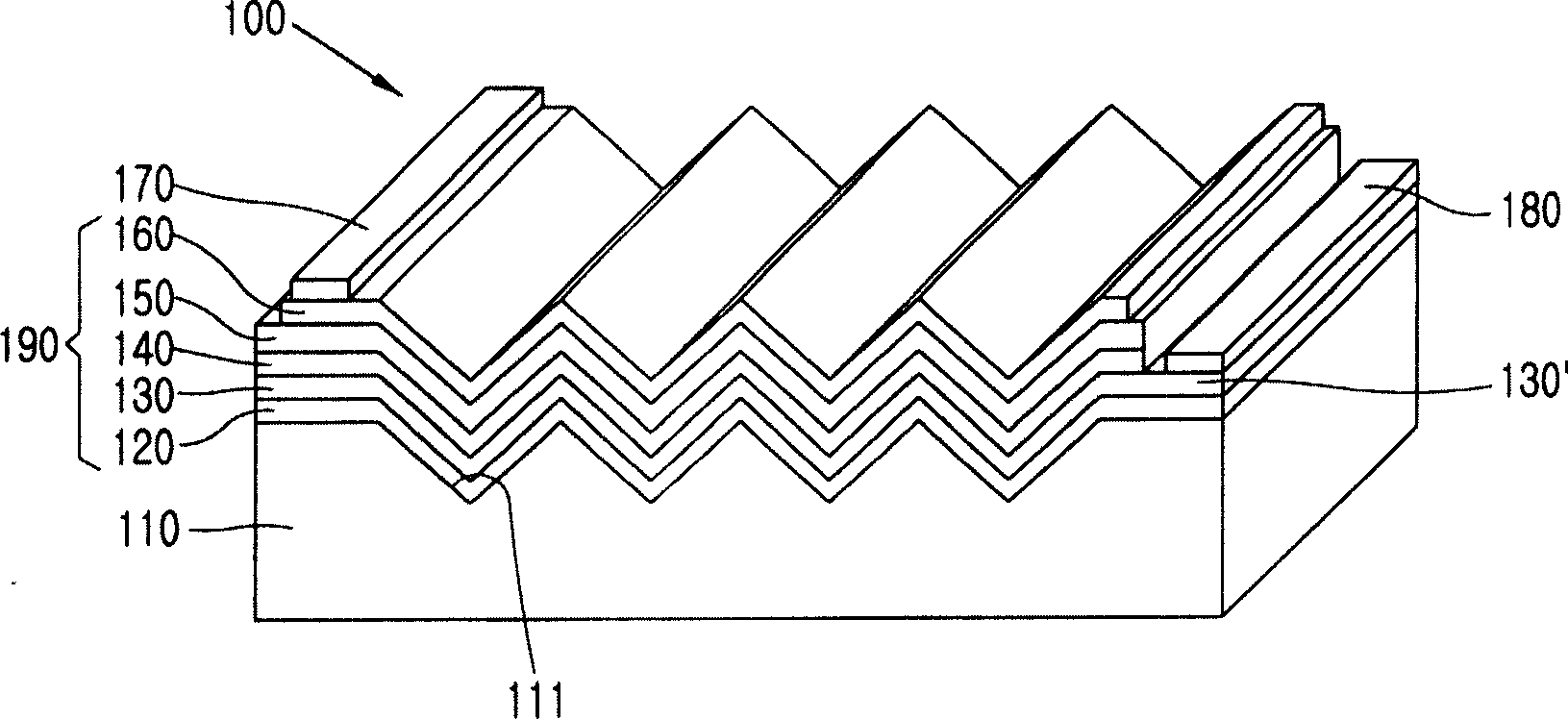
[0028] figure 2 Shown is a perspective view of a light emitting device according to a first embodiment of the present invention.

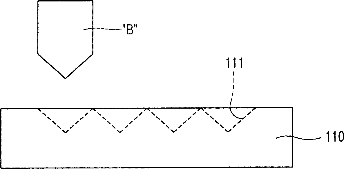
[0029] As shown in the figure, in the light emitting device 100 according to the first embodiment of the present invention, a groove having a 'V'-shaped cross section is formed on the upper surface of the substrate 110 by a half cut dicing method. portion 111, and then by forming the semiconductor layer 190 on the upper surface of the groove portion 111, the light emitting area of ​​the active layer 140 is increased, thereby improving the light emitting efficiency.

[0030] The light-emitting device 100 according to the first embodiment of the pre...


PUM


Abstract

The invention discloses a light emitting device and a manufacturing method thereof. A groove is formed on the substrate of the light-emitting device, and a buffer layer, an n-contact layer and an active layer are sequentially deposited on the groove, thereby increasing the light-emitting area of ​​the active layer. Therefore, the luminous efficiency is improved, and high-brightness light can be obtained with a substrate of the same size, thereby reducing production costs.

Description

technical field [0001] The present invention relates to a light-emitting device and a manufacturing method thereof, in particular to a light-emitting device capable of improving luminous efficiency by increasing the light-emitting area of ​​an active layer deposited on the upper surface of a substrate and a manufacturing method thereof. Background technique [0002] Currently widely used light emitting devices can be roughly classified into laser diodes (LDs) and light emitting diodes (LEDs). [0003] LDs are widely used as light sources in the field of optical communications. Recently, LDs are used in devices such as compact disc (CD) playback devices and compact disc record-playback devices (CD-RW), as well as DVD playback devices, laser disc (LD) playback devices, mini-disc (MD) playback devices etc. in the field of optical media. [0004] LEDs are used as common display devices, and also as backlight sources for light emitting devices or LCD display devices. [0005] ...

Claims


Application Information

Patent Timeline
IPC IPC(8): H01L33/12H01L33/14H01L33/42
CPCH01L33/24
Inventor 金根浩宋基彰
Owner LG ELECTRONICS INC
Why Eureka
Try Eureka