
Production of direct brazing filler metal button by double electrothermal filament smelting and cutting method

A manufacturing method and heating wire technology, which are applied to circuits, electrical components, electrical solid devices, etc., can solve the problems of many processes, complicated and bulky equipment, and high production costs.

Inactive Publication Date: 2005-07-27
HARBIN INST OF TECH
View PDF0 Cites 0 Cited by
  • Summary
  • Abstract
  • Description
  • Claims
  • Application Information

AI Technical Summary

Problems solved by technology

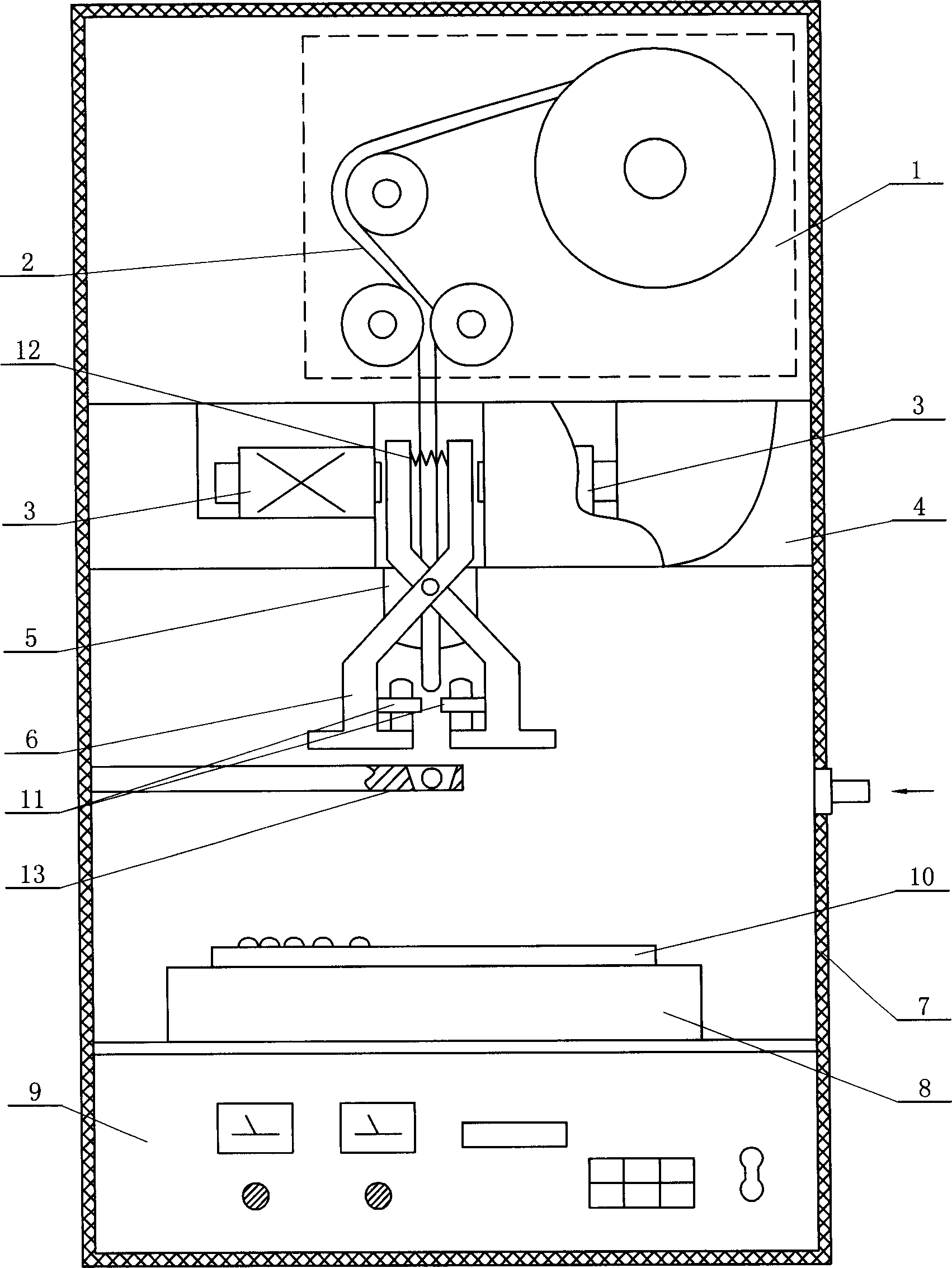
[0003] In order to overcome the defects of the existing bump manufacturing method with many processes, complicated and bulky equipment, and high production cost, a double heating wire fusion-cutting direct solder bump with fewer processes, simple equipment required, and low production cost is provided. Production Method

Method used


Image

  • Production of direct brazing filler metal button by double electrothermal filament smelting and cutting method
  • Production of direct brazing filler metal button by double electrothermal filament smelting and cutting method

Examples


Embodiment Construction

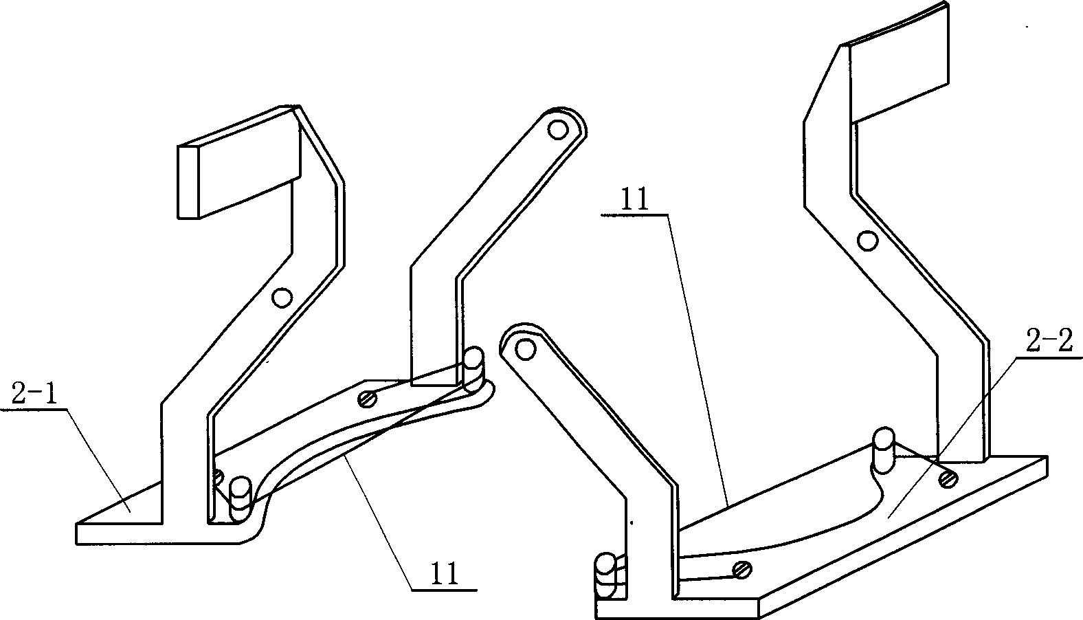
[0005] This embodiment is realized by the following steps: 1. By adjusting the position of the stage 8 on the horizontal plane, the substrate pad 10 fixed on the stage 8 is moved to the position where the bump needs to be made and aligned on the substrate The solder wire 2 above the pad 10 and the guide positioning funnel 13; two, the solder wire 2 is fed vertically downwards, so that the lower end of the solder wire 2 passes between two heating wires 11 arranged in parallel in the horizontal direction, Two heating wires 11 are connected in parallel on the power supply; three, two heating wires 11 are brought together and then separated, and the lower end of the solder wire 2 is fused and melted into molten drops and then drops through the guiding positioning funnel 13 to drop on the On the substrate pad 10, the droplet heats the substrate pad 10 and forms a bump connection with it; repeating the above three steps can complete the production of bumps on the entire substrate pad...


PUM


Abstract

The method includes following steps: 1, through the positional adjustment in the direction of horizontal on the objective table, the basal plate bonding pad fixed on the objective table is moved to the place where salient point is made, and aims at solder wire and guiding positional funnel; 2, the solder wire is vertically moved downward for making the bottom part of solder wire thread the place between the two heating wires. 3, the two heating wires close, and then open to make the bottom of solder wire melt; the molten drop is dropped on the basal plate bonding pad through the funnel to form the salient point.

Description

Technical field: [0001] The invention relates to a method for manufacturing bumps of an integrated circuit chip surface array package. Background technique: [0002] Due to the low-cost, high-speed, and multi-functional development of integrated circuits, the electronic packaging form has been transformed from the traditional packaging form to the new area array packaging. Area array packaging mainly includes ball grid array packaging (BGA) and chip scale packaging (CSP). Area array packaging technology has been widely used in all aspects of microelectronic packaging due to its excellent process performance and technical characteristics. The characteristic of the area array package is that spherical bumps are made in an array on the entire surface of the substrate as pins. How to find a method of making bumps that can provide reliable connections and have cost advantages has become the key to the research of packaging technology. The existing bump manufacturing technologi...

Claims


Application Information

Patent Timeline
Patent Type & Authority Applications(China)
IPC IPC(8): H01L21/60
CPCH01L2924/0002
Inventor 孔令超王春青李福泉田艳红
Owner HARBIN INST OF TECH
Learn More