This helps you quickly interpret patents by identifying the three key elements:
Problems solved by technology
Method used
Benefits of technology
Problems solved by technology
However, the precision offered by screen printing is no longer sufficient once attempts are made to reduce the size of the quiet zone reserved for the connection technique in order to optimize the surface of the display area of the component or to solve the problem of bulkiness
Method used
Image
Click on the blue label to locate the original text in one second.
Reading with bidirectional positioning of images and text.
Examples
Embodiment Construction
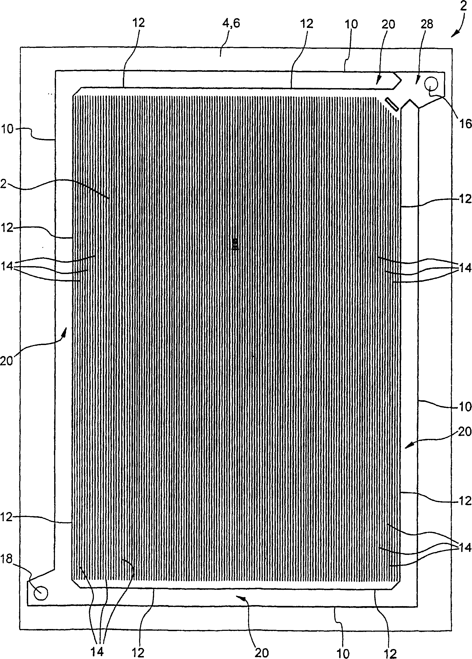
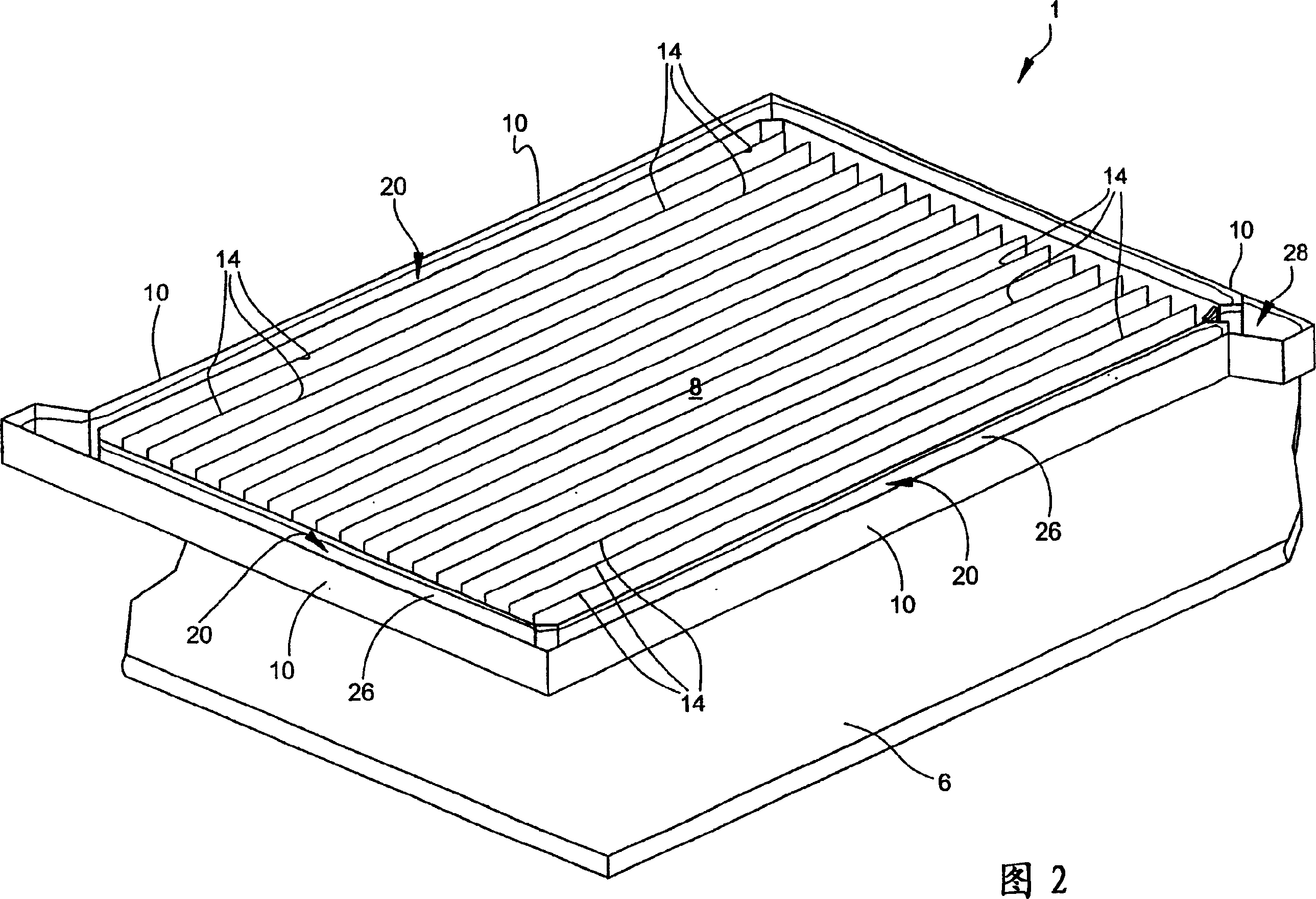
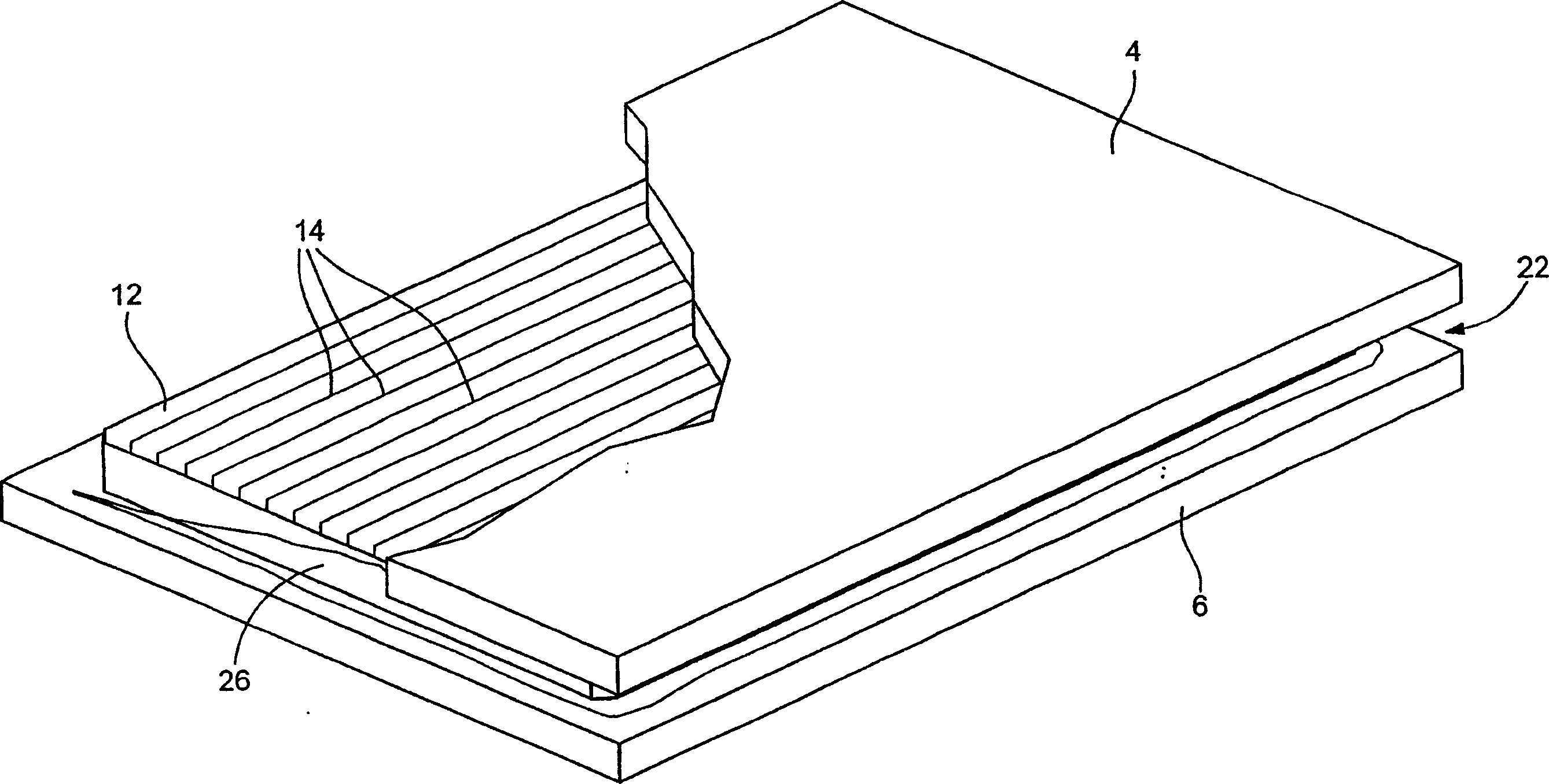
[0050] The present invention proceeds from the general inventive idea by proposing a new method of manufacturing a sealing frame which usually joins the bottom and top substrates of a display element, in particular a liquid crystal element, or an electrochemical optoelectronic element. According to the new method, the technique of depositing the sealing frame by screen printing, which usually takes place in the pre-component manufacturing stage and generates mechanical stresses that are detrimental to the already deposited adjacent component structures, is replaced by photolithography. The technique does not create any special stresses and in particular enables the simultaneous formation of the liner and the filling channel receiving the fluid sealing material which, after curing, forms the desired sealing frame. The invention also provides a new technique for assembling and sealing substrates of fluidic microsystems.
[0051] The invention will be described in connection with...
PUM
Abstract
The invention relates to a method for production of at least one device (2, 30, 48), defining a volume (8), for retaining a fluid or a sensitive material susceptible to a change in physical properties, particularly optical properties under the effect of application of a voltage, or in electrical properties under the effect of the application of a constraint or an irradiation. Said device (2, 30, 48) comprises at least one first front substrate (4, 38, 56) and at least one second rear substrate (6, 32, 50) held at a constant distance from each other, said two substrates (6, 32, 50; 4, 38, 56) being connected by a sealed joint (24, 46, 72) which defines the retention volume (8) for the sensitive material or fluid. The method is characterised in comprising the following steps: forming the structure of at least one septum (12, 44, 66) on one of the substrates (6, 32, 50) which defines the volume (8) for retention of the sensitive medium or fluid with the internal lateral face thereof, bringing the second substrate (4, 38, 56) together with the first substrate (6, 32, 50), introduction of a jointing material which can run into the gap (22), defined by the lateral external face of the septum (12, 44, 66) and the two superimposed substrates (6, 32, 50; 4, 38, 56) until at least a part of the volume of said gap (22) is occupied by the sealing material and solidification of the sealing material such as to generate the sealing joint (26, 46, 72).
Description
technical field [0001] The invention relates to a method of manufacturing devices such as electro-optic display elements or electrochemical optoelectronic elements. The present invention also relates to a specific type of microsystems known as "microelectromechanical systems" or "MEMS". Background technique [0002] The first known photovoltaic elements convert light into electricity by exploiting the photovoltaic effect that occurs at junctions of semiconductor materials. Semiconductor materials perform the functions of light absorption and separation of generated charges (electrons and holes) at the same time. The material must be of high purity and free of any defects, otherwise the electrons and holes recombine before they can be separated. [0003] The present invention relates to a second type of optoelectronic elements, called electrochemical elements, comprising semiconductor materials that are generally insensitive to visible light due to their bandgap band widths...
Claims
Application Information
Patent Timeline
Application Date:The date an application was filed.
Publication Date:The date a patent or application was officially published.
First Publication Date:The earliest publication date of a patent with the same application number.
Issue Date:Publication date of the patent grant document.
PCT Entry Date:The Entry date of PCT National Phase.
Estimated Expiry Date:The statutory expiry date of a patent right according to the Patent Law, and it is the longest term of protection that the patent right can achieve without the termination of the patent right due to other reasons(Term extension factor has been taken into account ).
Invalid Date:Actual expiry date is based on effective date or publication date of legal transaction data of invalid patent.