Interference analysis method and interference analysis device

一种分析装置、干扰量的技术,应用在电子电路测试、仪器、电数字数据处理等方向

Inactive Publication Date: 2005-09-14
PANASONIC CORP
View PDF1 Cites 0 Cited by
  • Summary
  • Abstract
  • Description
  • Claims
  • Application Information

AI Technical Summary

Problems solved by technology

However, with the method described in JP-A-2000-035984, it is also difficult to analyze the interference between wirings on a circuit board with a complicated structure.

Method used


Image

  • Interference analysis method and interference analysis device
  • Interference analysis method and interference analysis device
  • Interference analysis method and interference analysis device

Examples


Embodiment approach 1

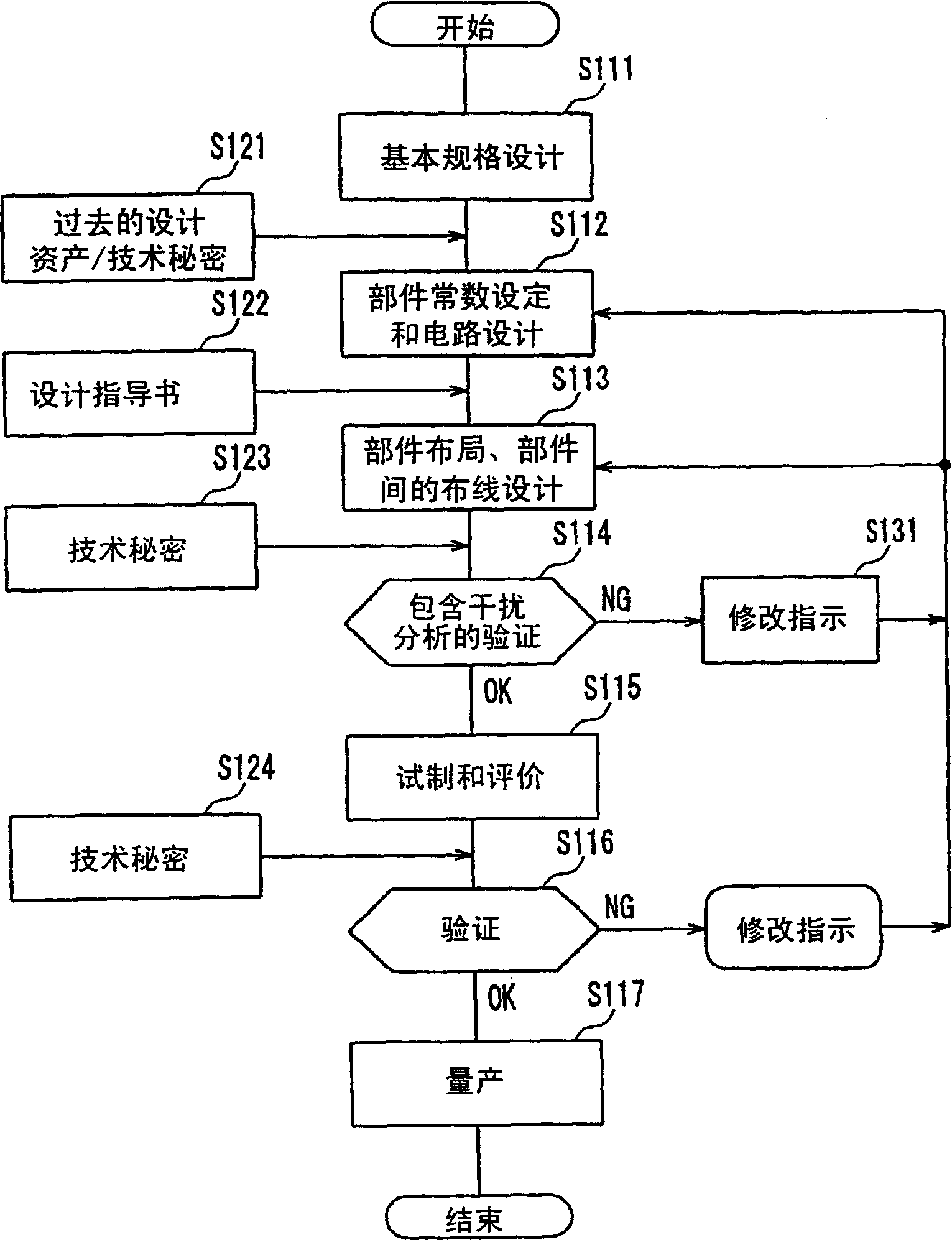
[0085] Embodiment 1 relates to an interference analysis method and an interference analysis device for greatly reducing the design load of a high-frequency circuit, a program for causing a computer to execute processing for realizing the interference analysis method and the interference analysis device, and a recording medium recording the program.

[0086] figure 1 It is a flowchart of a schematic procedure of high-frequency circuit design performed by the interference analysis method of this embodiment.

[0087] figure 1 The schematic procedure shown is in many respects the same as the conventional digital circuit design schematic procedure shown in FIG. 9 , so the same parts will be briefly described, and the different parts will be described in detail.

[0088] At the beginning of this design, the design of the basic specifications is performed first (S111). In the design of the basic specifications, the basic matters when selecting or determining the specifications re...


PUM


Abstract

The present invention relates to a method and a device for analyzing mutual interference between wirings formed on a circuit board by electromagnetic induction using a computer, and analyzing the interference between wirings in a high-frequency circuit in a short time with a low load. The interference analysis device includes: a design data input unit (411), which inputs design data of the circuit board; a noise characteristic setting unit (413), which sets data representing electrical characteristics of noise of wiring formed on the circuit board; a limit value The setting part (414) sets the allowable limit value of the noise received by the wiring; the selection part (415) selects the wiring group of the analysis object according to the noise characteristic data and the allowable limit value; the interference analysis part (416) selects In the wiring group, calculate the interference amount from the interfering wiring to the disturbed wiring; and the reception noise level calculation part (420) calculates the noise level received by the disturbed wiring based on the interference amount and noise characteristic data .

Description

technical field [0001] The present invention relates to a method and device for analyzing mutual interference caused by electromagnetic induction between wirings formed on a circuit board by using a computer, and for investigating its influence, or a program for causing a computer to execute the process, and a record for recording the program medium. Background technique [0002] Among the existing methods and devices for analyzing the mutual interference caused by electromagnetic induction between the wirings formed on the circuit board with a computer and investigating its influence, there is, for example, the noise described in (Japanese) Unexamined Patent Publication No. 2000-035984 Inspection methods and devices. [0003] FIG. 9 is a flowchart of a schematic procedure of conventional digital circuit design. [0004] At the beginning of this design, the design of the basic specifications is performed first (S911). In the design of basic specifications, without touchin...

Claims


Application Information

Patent Timeline
Patent Type & Authority Applications(China)
IPC IPC(8): G01R31/28G06F17/50H01L21/82
CPCG06F17/5036G06F30/367
Inventor 岩城秀树小掠哲义小松直树中山武司木下智博
Owner PANASONIC CORP
Why Eureka
Try Eureka