Wiring substrate, solid-state imaging apparatus using the same, and manufacturing method thereof

A wiring substrate and imaging lens technology, applied in the field of solid-state imaging devices, can solve problems such as hindering the miniaturization of the solid-state imaging device 100

Inactive Publication Date: 2005-09-28
SAMSUNG ELECTRONICS CO LTD
View PDF1 Cites 9 Cited by
  • Summary
  • Abstract
  • Description
  • Claims
  • Application Information

AI Technical Summary

Problems solved by technology

[0009] When the passive element 120 is installed in the solid-state imaging device 100, refer to figure 1 , the horizontal length (L1) of the solid-state imaging device 100 is increased, thereby hindering the miniaturization of the solid-state imaging device 100

Method used


Image

  • Wiring substrate, solid-state imaging apparatus using the same, and manufacturing method thereof
  • Wiring substrate, solid-state imaging apparatus using the same, and manufacturing method thereof
  • Wiring substrate, solid-state imaging apparatus using the same, and manufacturing method thereof

Examples


Embodiment Construction

[0028] Advantages and features of the present invention, and methods for implementing the present invention will be more easily understood by referring to the following detailed description of the preferred embodiments and accompanying drawings. However, the invention may be embodied in many different forms and should not be construed as limited to the embodiments set forth herein. Rather, these embodiments are provided so that this disclosure will be thorough and complete, and will fully convey the scope of the various embodiments of the invention to those skilled in the art. The scope of the invention is limited only by the appended claims. Like reference numerals refer to like elements throughout the specification and drawings.

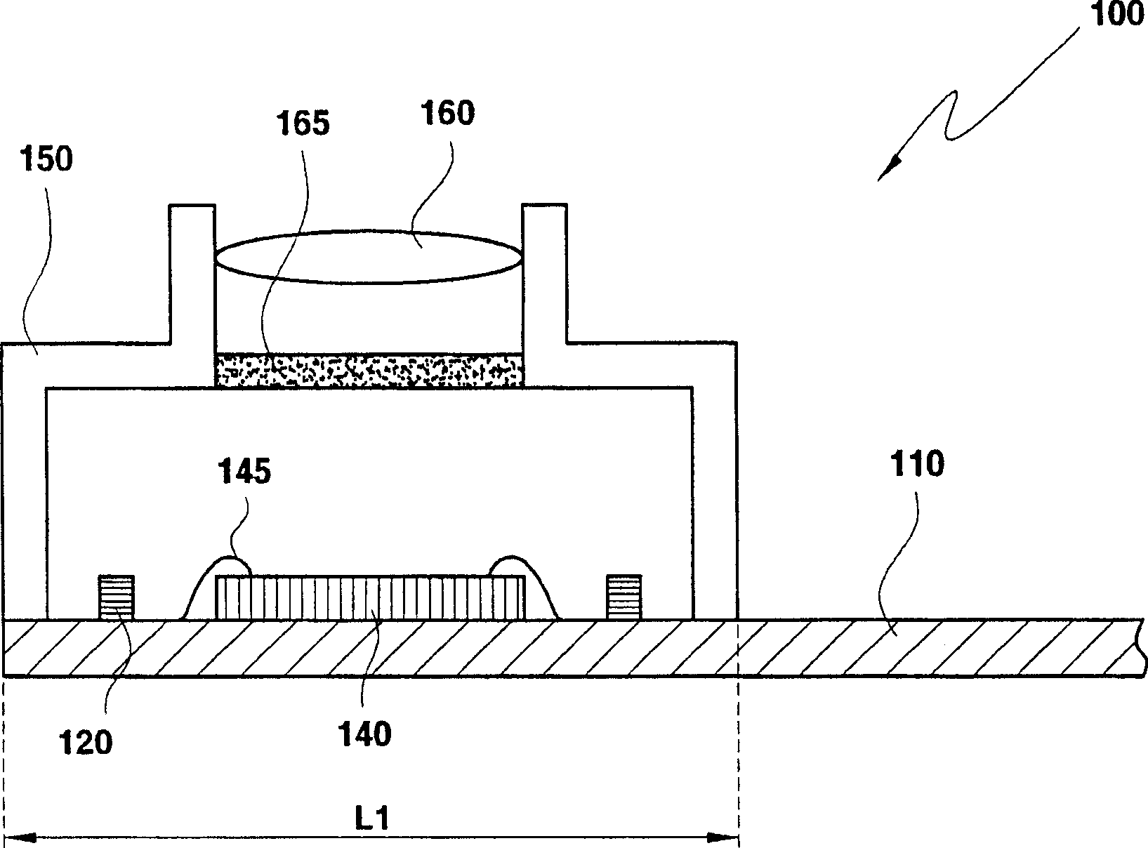
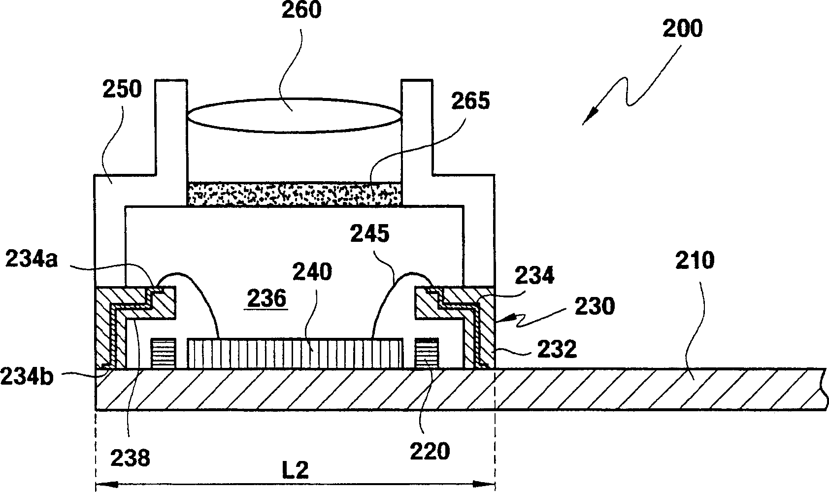
[0029] refer to Figures 2A to 4E , Embodiments of the present invention will now be described.

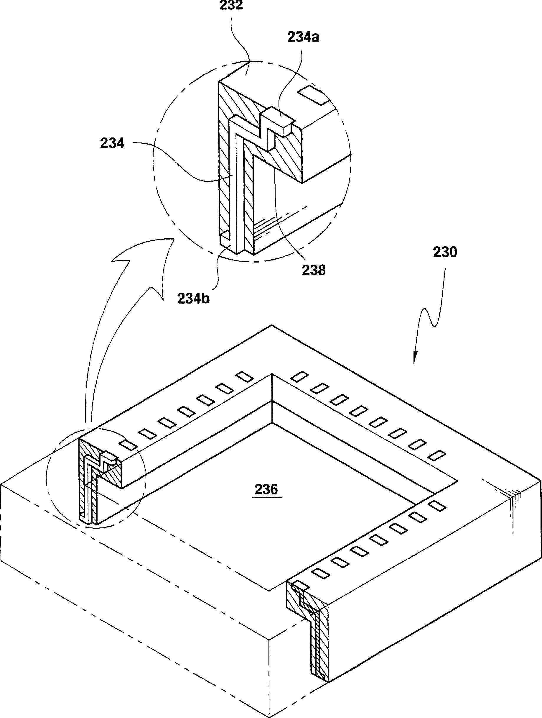
[0030] Figure 2A is a cross-sectional view of the solid-state imaging device 200, and Figure 2B is shown in Figure 2A A partially exploded pe...


PUM


Abstract

In one embodiment, a miniaturized solid-state imaging apparatus includes a body having a cavity for mounting a semiconductor chip therein. The body has an overhanging portion extending toward the cavity. Further, a lead is disposed within the body. The lead has one end exposed through a top surface of the body and the other end exposed through a bottom surface of the body for electrical connection thereof.

Description

[0001] This application claims priority from Korean Patent Application No. 10-2004-0009029 filed with the Korean Intellectual Property Office on February 11, 2004, the disclosure of which is incorporated herein by reference in its entirety. technical field [0002] The present invention relates to a solid-state imaging device, and more particularly, to a solid-state imaging device in which a semiconductor chip has a first wiring substrate electrically coupled between a lens member and a second wiring substrate. Background technique [0003] Generally, a mobile electronic device, such as a personal digital assistant (PDA), a digital camera (DSC), or a mobile phone, has an embedded solid-state imaging device in which a semiconductor chip is combined with a lens. In a mobile phone equipped with a small digital camera, an image of a calling user is picked up by the camera and input to the mobile phone as image data, and the input image data can be transmitted to the called user. ...

Claims


Application Information

Patent Timeline
Patent Type & Authority Applications(China)
IPC IPC(8): H01L27/14H01L23/00H01L23/02H01L23/04H01L23/12H01L23/50H01L27/146H01L27/148H01L31/0203H01L31/0232H04N5/225H04N5/335
CPCH04N5/2251H01L27/14806H01L31/0203H01L27/14618H04N5/2254H01L2224/49171H01L31/0232H04N5/2253H01L31/02325H01L27/14625H04N23/54H04N23/55H01L2224/48091H01L2924/00014G01R1/07328G09G3/006
Inventor 曹民教都载天权宁信
Owner SAMSUNG ELECTRONICS CO LTD
Why Eureka
Try Eureka