
Poly(azine)-based charge transport materials
A charge transport and photoconductive technology, applied in the field of polymer charge transport materials, can solve the problems of large charge transport materials and harmful organic photoreceptor performance, and achieve high-quality results
- Summary
- Abstract
- Description
- Claims
- Application Information
AI Technical Summary
Problems solved by technology
Method used
Image

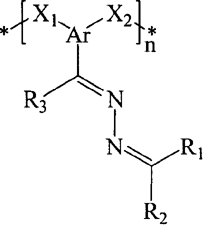
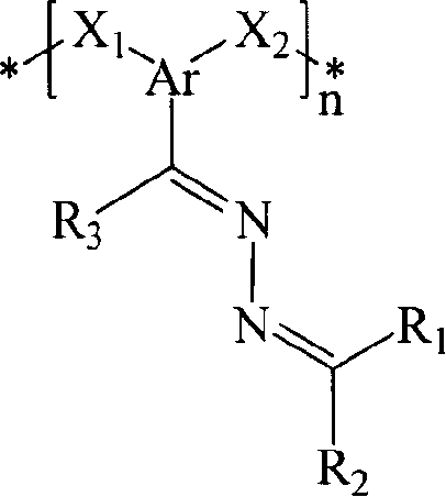
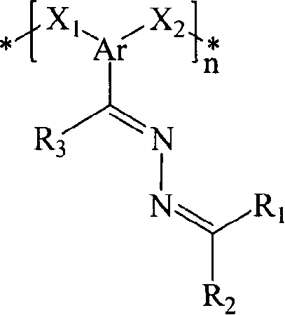
Examples
Embodiment 1-
[0116] Example 1- Synthesis and Characterization of Charge Transport Materials
[0117] This example describes the synthesis and characterization of compound (1). Characterization includes chemical characterization of the compound. And the electrostatic properties of materials formed from said compounds, such as mobility and ionization potential, are described in the subsequent examples.
[0118] Bis(4,4′-diethylamino)benzophenone hydrazone
[0119] Bis(4,4'-diethylamino)benzophenone (108.1 g, 0.335 mol, obtained from Aldrich), hydrazine monohydrate (98%, 244 ml, 5 mol, obtained from Aldrich) in 250 ml 2-propanol ) and 10 ml of concentrated hydrochloric acid (obtained from Aldrich) were added to a 1000 ml three-necked round bottom flask equipped with a reflux condenser and a mechanical stirrer. With vigorous stirring, the solution was refluxed for about 6 hours until bis(4,4'-diethylamino)benzophenone disappeared. The solution was left to stand overnight. Crystals for...
Embodiment 2-
[0126] Example 2- Measuring Charge Mobility
[0127] This example describes the measurement of the charge mobility and ionization potential of charge transport materials, in particular the charge mobility and ionization potential of compound (1) described above.
[0128] Sample 1
[0129] A mixture of 0.1 g of compound (1) and 0.1 g of polycarbonate Z was dissolved in 2 ml of tetrahydrofuran. The solution was applied to a polyester film with a conductive aluminum layer by means of a dip roller. When the coating was dried at 80° C. for 1 hour, a 10 μm thick transparent layer was formed. The hole mobility of the samples was measured, and the results are listed in Table 1.
[0130] Measuring Mobility
[0131] Each sample was positively corona charged until the surface potential was U and irradiated with 2 ns long nitrogen laser pulses. Hole mobility μ was measured according to Kalade et al., "Investigation of charge carrier transferin electrophotographic layers of chal...
Embodiment 3
[0135] Example 3 - Measurement of ionization potential
[0136] This example describes the measurement of the ionization potential of the charge transport material described in Example 1.
[0137] To measure the ionization potential, a solution of 2 mg of charge transport material in 0.2 ml of tetrahydrofuran was placed at 20 cm 2 A thin layer of charge transport material about 0.5 μm thick is coated on the surface of the substrate. The substrate was an aluminized polyester film coated with a 0.4 μm thick sublayer of methylcellulose.
[0138] According to the method described by Grigalevicius et al. in "3,6-Di(N-diphenylamino)-9-phenylcarbazole and its methyl-substituted derivative as novel hole-transporting amorphous molecular materials" Synthetic Metals 128 (2002), Pp.127-131 The ionization potential was measured, which document is incorporated herein by reference. Specifically, each sample was illuminated with monochromatic light from a quartz monochromator with a deuter...
PUM
| Property | Measurement | Unit |
|---|---|---|
| resonance energy | aaaaa | aaaaa |
| resonance energy | aaaaa | aaaaa |
| melting point | aaaaa | aaaaa |
Abstract
Description
Claims
Application Information