Supercharge Your Innovation With Domain-Expert AI Agents!

Display device producing method and display device producing device

A technology for display devices and manufacturing equipment, which is applied in optics, instruments, discharge tubes, etc., and can solve problems such as light transmission and adverse effects on image quality.

Inactive Publication Date: 2005-11-16
SONY GRP CORP
View PDF0 Cites 4 Cited by
  • Summary
  • Abstract
  • Description
  • Claims
  • Application Information

AI Technical Summary

Problems solved by technology

However, there may be situations where misalignment around the spacer during operation adversely affects the image quality, for example, light break-through occurs, or the spacer can be visually observed

Method used


Image

  • Display device producing method and display device producing device
  • Display device producing method and display device producing device
  • Display device producing method and display device producing device

Examples


no. 1 example

[0023] The first embodiment of the present invention will be described below by referring to the drawings.

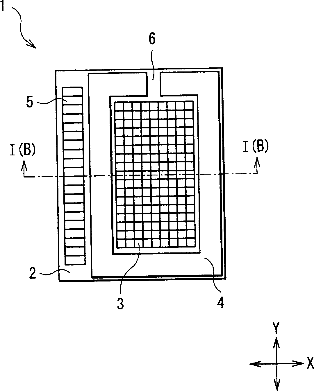
[0024] First, refer to Figure 1A with 1B The structure of the display device according to the embodiment of the present invention will be described below.

[0025] Figure 1A with 1B The structure of the display panel 1 is shown, which is the main part of the display device according to the present embodiment. Figure 1A Shows a plan view directly from above, and Figure 1B Is along the arrow direction Figure 1A A cross-sectional view taken from the line I(B)-I(B). The display panel 1 is formed as an active matrix reflective liquid crystal display device. in Figure 1A In order to facilitate understanding, the top substrate 7 is shown (which will be described below).

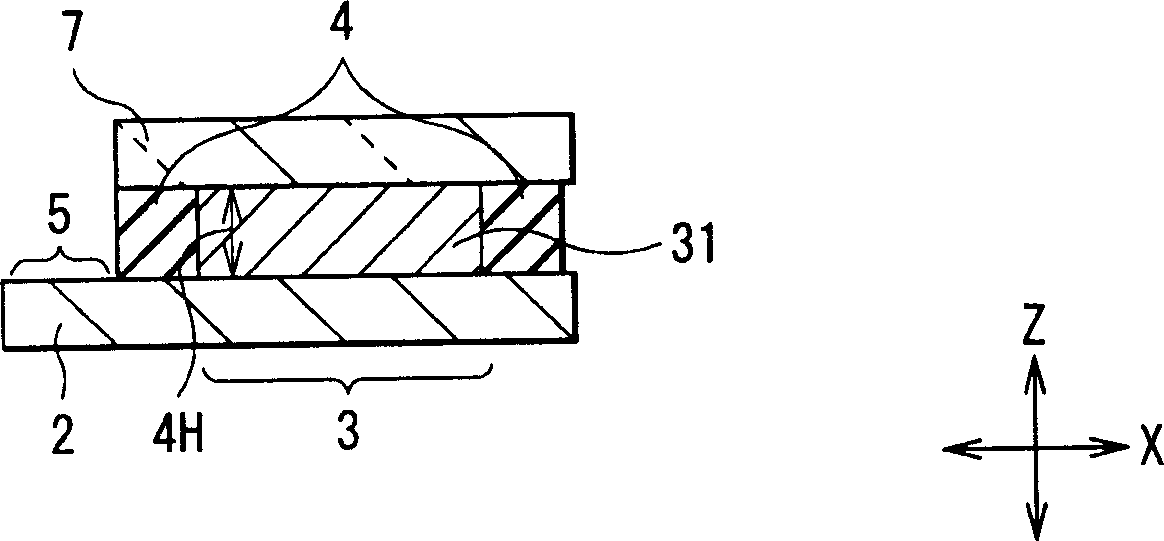
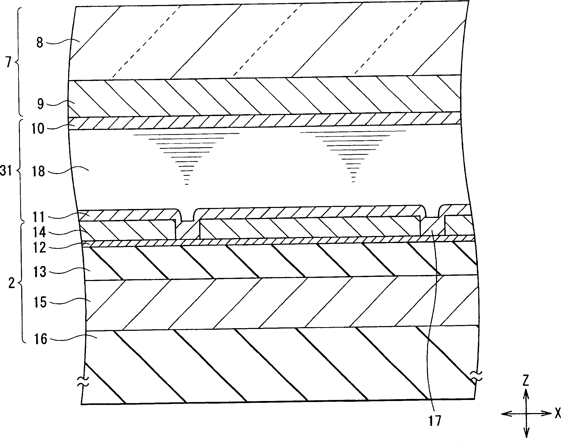
[0026] Such as Figure 1A with 1B As shown, the display panel 1 includes a rectangular bottom substrate 2 and a rectangular top substrate 7, and a display portion 31 and a sealing pattern 4 sandwiched betw...

no. 2 example

[0062] Below, reference Figure 11A with 11B In the following, a method of manufacturing a display device and a display device manufacturing apparatus according to a second embodiment of the present invention will be described.

[0063] Figure 11A with 11B The bonding apparatus according to the present embodiment is shown as a display device manufacturing apparatus, and is similar to that in the first embodiment Figure 5A with Figure 5B Corresponding. Such as Figure 5A with 5B Case, Figure 11A Shows the open state before pressure is applied, and Figure 11B Shows the state of applying pressure. in Figure 11A with 11B In, the same components are used with Figure 5A with 5B The same reference numerals are used for identification.

[0064] In the following description, the main differences between the display device manufacturing method and display device manufacturing apparatus according to this embodiment and the first embodiment will be described below, and other points wil...


PUM

PropertyMeasurementUnit
roughnessaaaaaaaaaa
roughnessaaaaaaaaaa

Abstract

Provided are a manufacturing method which can efficiently manufacture a display device with higher image quality, and a manufacturing apparatus which can be applied to the manufacturing method. Position adjustment is carried out so that a seal pattern (4) formed on at least one of a bottom substrate (2) and a top substrate (7) and having a shape along an outer edge of each of a plurality of display panels (1) coincides with a projected portion pattern (27) (29) formed on at least one of a pair of parallel surfaces (19S) (20S) in a bottom surface plate (19) and a top surface plate (20) and having a planar shape corresponding to the seal pattern (4), and pressure is applied to the bottom substrate (2) and the top substrate (7) in a Z direction by the bottom surface plate (19) and the top surface plate (20). Therefore, a gap between the bottom substrate (2) and the top substrate (7) in an effective screen area (3) can be formed more uniformly, and a display device with higher image quality can be efficiently manufactured.

Description

Technical field [0001] The present invention relates to a method of manufacturing a display device capable of displaying high-quality images, and a display device manufacturing equipment used in the method of manufacturing the display device. Background technique [0002] In recent years, there has been an increasing demand for reductions in weight and appearance of electronic display devices. Various electronic display devices such as light emitting diodes (LED), plasma display panels (PDP) and liquid crystal displays (LCD) have been available Developed. [0003] Among the electronic display devices, LCDs in particular have characteristics such as high image quality, small outline, light weight, and low power consumption, and LCDs are used in a large number of final products such as clocks, televisions, personal computers, and projectors. Compared with other electronic display devices, it is used in various applications. For example, a typical LCD has a structure in which a liqu...

Claims


Application Information

Patent Timeline
Patent Type & Authority Applications(China)
IPC IPC(8): G02F1/1333G02F1/1339
CPCG02F1/1339G02F2001/133354H01J2211/36G02F1/133354G02F1/13
Inventor 清宫正桥本俊一
Owner SONY GRP CORP
Features
  • R&D
  • Intellectual Property
  • Life Sciences
  • Materials
  • Tech Scout
  • Unparalleled Data Quality
  • Higher Quality Content
  • 60% Fewer Hallucinations
Learn More