
Inspector for surface deficiency of silicon sheet with scattered light intensity doubling system

A silicon wafer surface, scattered light technology, applied in the direction of instruments, measuring devices, scientific instruments, etc., can solve the problems of insufficient concentration of scattered signals, influence, unfavorable collection of scattered light, etc., and achieve the effect of avoiding interference

Inactive Publication Date: 2005-12-28
SHANGHAI INST OF OPTICS & FINE MECHANICS CHINESE ACAD OF SCI
View PDF0 Cites 10 Cited by
  • Summary
  • Abstract
  • Description
  • Claims
  • Application Information

AI Technical Summary

Problems solved by technology

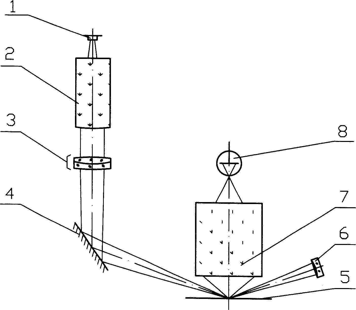
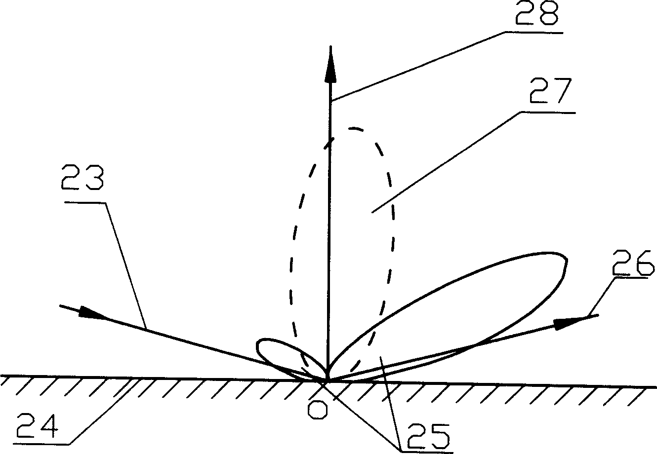
In addition, the theory shows that the scattering signal on the reflected light side of the fine particle is much stronger than the incident light side, such as image 3 As shown in , while in the prior art, the two focuses are incident from both sides, so the defect scattering signal is not concentrated enough, which is not conducive to the collection of scattered light
and in figure 1 The condenser lens group in the device is located in the normal direction of the surface of the silicon wafer (5) to be measured, and is easily affected by the surface scattering signal in the normal direction

Method used


Image

  • Inspector for surface deficiency of silicon sheet with scattered light intensity doubling system
  • Inspector for surface deficiency of silicon sheet with scattered light intensity doubling system
  • Inspector for surface deficiency of silicon sheet with scattered light intensity doubling system

Examples


Embodiment Construction

[0022] The present invention is described in detail below in conjunction with accompanying drawing.

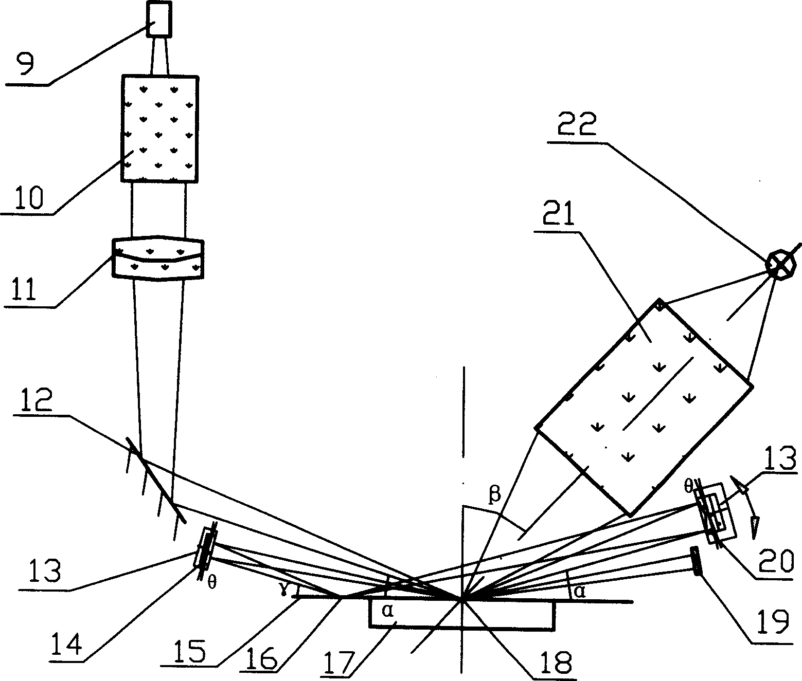
[0023] see first figure 2 , figure 2 It is a schematic diagram of the system of the present invention. As can be seen from the figure, the present invention has a silicon wafer surface defect detector with a scattered light intensity multiplication system, including a laser incident system and a defect scattered light collection system. The laser incident system consists of a laser 9, a beam expander system 10, a focusing mirror 11 and Plane reflector 12 is formed, and described defective scattered light collection system is made up of a condenser lens group 21 and is positioned at the focus position photodetector 22 of this condenser lens group 21, is characterized in that also has:

[0024] 1. The scattered light intensity multiplication system is made up of the first spherical reflector 20 and the second spherical reflector 14, and its positional relationship is: the li...


PUM


Abstract

A detector of detect on silicon wafer surface is featured as forming multiplier system of scattering light intensity by the first and the second spherical mirrors with a light trap and on a light axis regulating frame, presenting light axis of defect scattering light collection system in included angle beta to normal of silicon wafer to be detected and moving detected silicon wafer in plane and in rotation by operation table to let two spherical mirrors, trap and planar reflector satisfy to object - image relation of geometrical optics.

Description

technical field [0001] The invention is related to silicon chip surface defect detection, in particular to a silicon chip surface defect detector with a scattered light intensity multiplication system, which uses the Mie scattering principle to detect real-time defects on the silicon chip surface in integrated circuit manufacturing. Background technique [0002] In recent years, laser scanning scattering detection technology for various surface defects has been developed rapidly. When a focused laser beam is scanned across the surface of a silicon wafer, defects on the surface generate defect-scattered light. The scattered light of these defects contains abundant information such as the shape, type and position of the defects. The light scattered by these defects is collected by photodetectors, analyzed and processed, and signals such as the shape and position of the defects are finally obtained. [0003] Existing silicon wafer surface defect detection systems such as fig...

Claims


Application Information

Patent Timeline
Patent Type & Authority Applications(China)
IPC IPC(8): G01N21/956
Inventor 张志平程兆谷高海军覃兆宇
Owner SHANGHAI INST OF OPTICS & FINE MECHANICS CHINESE ACAD OF SCI
Learn More