Exposure apparatus and method for producing device

An exposure device and optical path technology, which can be used in semiconductor/solid-state device manufacturing, photolithography process exposure devices, microlithography exposure equipment, etc. Occurs, suppresses the effects of poor exposure or bad shots

Inactive Publication Date: 2006-01-18
NIKON CORP
View PDF24 Cites 4 Cited by
  • Summary
  • Abstract
  • Description
  • Claims
  • Application Information

AI Technical Summary

Problems solved by technology

In this case, there is a possibility that the pattern image is not formed on the substrate, and if it is left as it is, no defect will be found until it becomes the final device, which may cause a decrease in productivity.
[0009] Furthermore, in the exposure apparatus using the liquid immersion method, there are cases where various measurements are performed via the liquid on the image plane side of the projection optical system. In the case of the situation, there is a possibility that a measurement error occurs or the state cannot be measured

Method used


Image

  • Exposure apparatus and method for producing device
  • Exposure apparatus and method for producing device
  • Exposure apparatus and method for producing device

Examples


Embodiment Construction

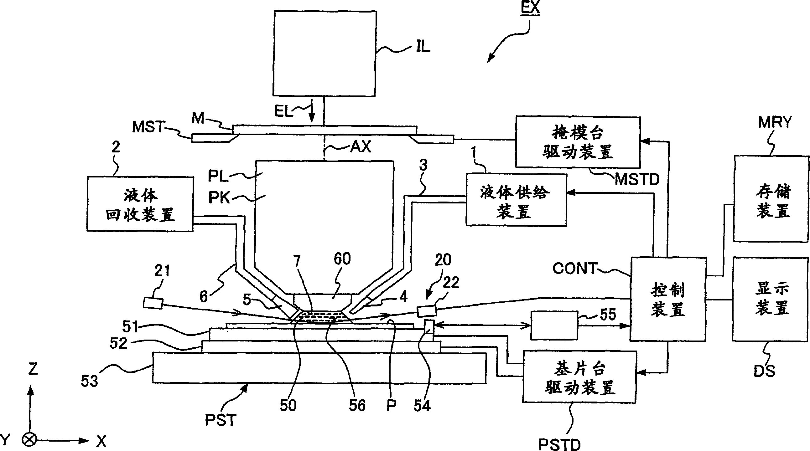
[0037] Hereinafter, with regard to the exposure apparatus and device manufacturing method of the present invention, refer to the attached Figure 1 While explaining, the present invention is not limited thereto. figure 1 It is a schematic configuration diagram showing one embodiment of the exposure apparatus of the present invention.

[0038] exist figure 1 Among them, the exposure apparatus EX includes: a mask stage MST supporting the mask M, a substrate stage PST supporting the substrate P, an illumination optical system IL for illuminating the mask M supported by the mask stage MST with exposure light EL, The projection optical system PL for projecting and exposing the pattern image of the mask M illuminated by the exposure light EL onto the substrate P supported by the substrate stage PST, and the control device CONT for collectively controlling the overall operation of the exposure device EX are connected to The control device CONT stores the storage device MRY of inf...


PUM

PropertyMeasurementUnit
refractive indexaaaaaaaaaa

Abstract

An exposure apparatus, wherein an exposure of a substrate (P) is carried out by filling at least a portion of the space between a projection optical system and the substrate (P) with a liquid and projecting an image of a pattern onto the substrate (P) via the projection optical system and the liquid, includes a bubble detector (20) which detects air bubble or bubbles in the liquid between the projection optical system and the substrate (P). Consequently, the exposure apparatus is capable of suppressing deterioration of a pattern image caused by bubbles in the liquid when an exposure is carried out while filling the space between the projection optical system and the substrate with the liquid.

Description

technical field [0001] The present invention relates to an exposure device for exposing a pattern image projected by a projection optical system in a state where at least a portion between the projection optical system and a substrate is filled with liquid, and a device manufacturing method using the exposure device. Background technique [0002] A semiconductor device or a liquid crystal display device is manufactured by a method called photolithography in which a pattern formed on a mask is transferred to a photosensitive substrate. The exposure apparatus used in this photolithography process has a mask stage that supports the mask and a substrate stage that supports the substrate. While moving the mask stage and the substrate stage one by one, the pattern of the mask is projected through the projection optical system. Transfer to substrate. In recent years, in order to cope with higher integration of device patterns, higher resolution of projection optical systems has be...

Claims


Application Information

Patent Timeline
Patent Type & Authority Applications(China)
IPC IPC(8): H01L21/027G03F7/20
Inventor 水谷英夫马込伸贵
Owner NIKON CORP
Why Eureka
Try Eureka