Circuit for configuring chip pins with multiplexing functions, and method for configuring chip pins with multiplexing functions

A technology for function multiplexing and configuring circuits, which is applied in the direction of lamp circuit layout, logic circuits, electric light sources, etc., can solve the problems of reliable configuration of chips that cannot work, inconvenient hardware design, and failure of configuration circuits, etc., to increase system reliability , increase cost, low cost effect

Active Publication Date: 2006-02-01
NEW H3C TECH CO LTD
View PDF0 Cites 20 Cited by
  • Summary
  • Abstract
  • Description
  • Claims
  • Application Information

AI Technical Summary

Problems solved by technology

[0010] 1. Inconvenient hardware design
Since the chip pins are fixed to "0" or "1", once the printed circuit board (PCB) is placed on the board, it cannot be changed, resulting in a certain default state inside the chip that cannot be changed by hardware after power-on.
At this time, if the configuration is wrong, or the default configuration state of the chip needs to be re-modified, it is necessary to temporarily change the hardware circuit, which is very inconvenient
[0011] 2. Poor circuit reliability
use figure 1 or figure 2 The design method, if the LED indicator is damaged, the configuration circuit will fail, and the chip cannot be reliably configured for its working mode when it is powered on

Method used


Image

  • Circuit for configuring chip pins with multiplexing functions, and method for configuring chip pins with multiplexing functions
  • Circuit for configuring chip pins with multiplexing functions, and method for configuring chip pins with multiplexing functions
  • Circuit for configuring chip pins with multiplexing functions, and method for configuring chip pins with multiplexing functions

Examples


Embodiment Construction

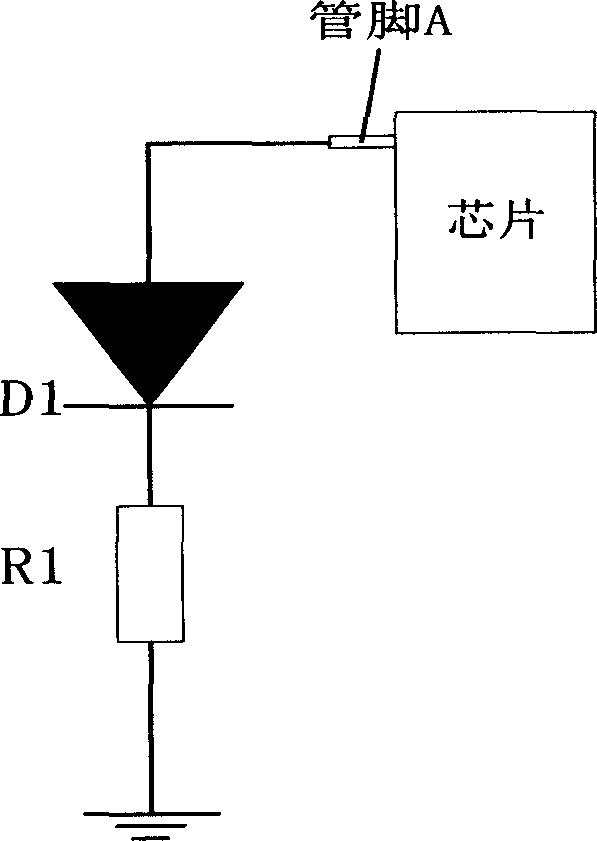
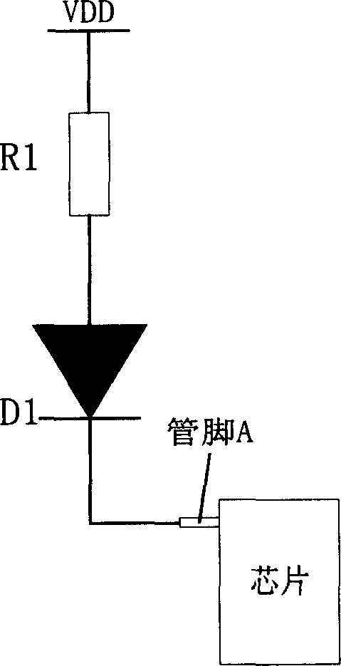
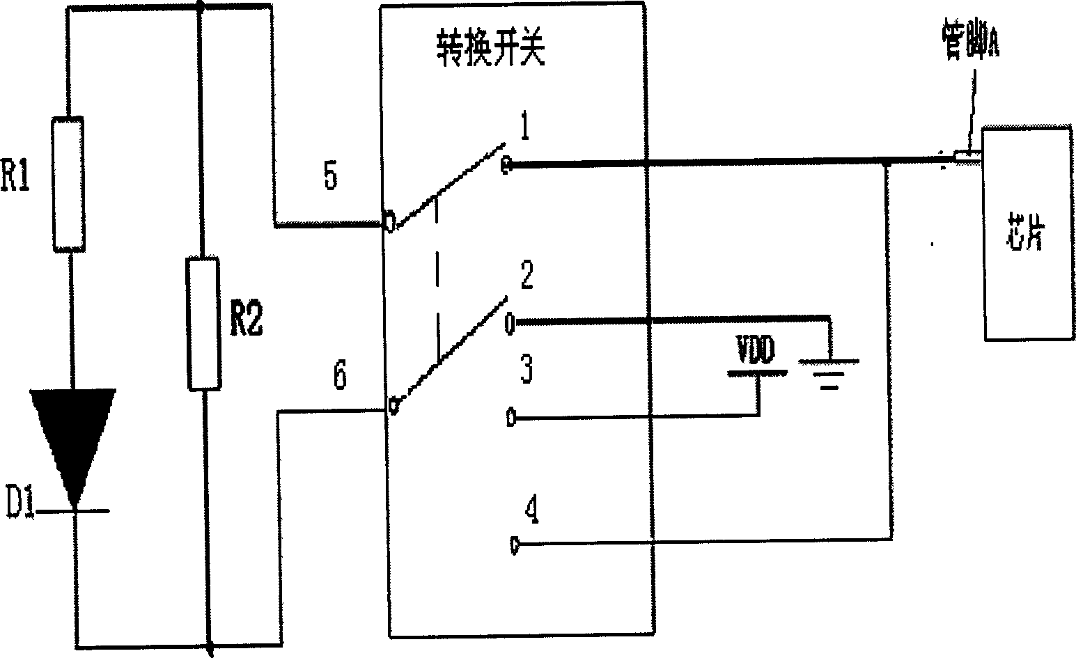
[0038] see Figure 4 , is the circuit diagram that the present invention adopts the bus switch to configure the pin A of the function multiplexing chip, including the pin A of the multiplexing chip, a current-limiting resistor R1 connected in series with each other, an LED indicator light D1, and a bypass resistor R2. The circuit is connected in parallel with the bypass resistor R2, and a bus switch includes the first group of channels A0 and B0, A1 and B1, the second group of channels A8 and B8, and A9 and B9, totaling two groups of four channels. and image 3 The connections shown correspond to each other. Pins A0 and A8, A1 and A9 respectively correspond to LED drive pins 5 and 6 of the original transfer switch, and pin B0 corresponds to the original power-on default configuration of "0" to control pins 1, Pin B9 corresponds to the original power-on default configuration as "1" to control pin 4, pin B1 corresponds to the original ground pin 2, and pin B8 corresponds to the...


PUM


Abstract

The configuration circuit includes circuit of LED indicator light, bypass resistor, alternation switch. The alternation switch includes two pieces of LED drive pins, control pin for setting up í«0í», control pin for setting up í«1í», grounding pin, and pin for setting up voltage. The circuit of LED indicator light is connected to LED drive pins of the alternation switch. Control pin for setting up í«0í» and control pin for setting up í«1í» are connected to same functional multiplexing pin A of a chip. Bypass resistor is connected to circuit of LED indicator light in parallel. If pin A is needed to be configured as í«0í», through the control alternation switch, LED drive pin and control pin for setting up í«0í» are connected to grounding pin. If pin A is needed to be configured as í«0í», through the control alternation switch, LED drive pin and control pin for setting up í«0í» are connected to pin for setting up voltage. The circuit is simple and reliable.

Description

technical field [0001] The invention relates to a configuration circuit, in particular to a flexible configuration circuit and a method for configuring function multiplexing chip pins in an Ethernet chip for communication. Background technique [0002] In the current Ethernet chips, the working mode of some chips can be configured through specific pins. In order to save costs in chip design, the configuration pins are often multiplexed with other pins. Foot reuse. At the initial stage of chip power-on, the pins play a configuration role, and after a period of stable power-on (generally about tens of milliseconds), the pins are used to drive the indicator light. The indicator lights generally use light-emitting diodes, and the driving mode of the indicator lights must be consistent with the power-on configuration of the pins. [0003] The working principle of the chip pin that multiplexes the two functions of default configuration and LED driving is as follows (assuming tha...

Claims


Application Information

Patent Timeline
Patent Type & Authority Applications(China)
IPC IPC(8): H03K19/00H05B37/02
Inventor 黄自亮李炜
Owner NEW H3C TECH CO LTD
Why Eureka
Try Eureka