Semiconductor apparatus

A semiconductor and power technology, which is applied in output power conversion devices, amplifier protection circuit layouts, logic circuits, etc., can solve problems such as difficulty in level determination of control integrated circuits and reducing the accuracy of open circuit levels.

Inactive Publication Date: 2006-03-01
MITSUBISHI ELECTRIC CORP
View PDF3 Cites 4 Cited by
  • Summary
  • Abstract
  • Description
  • Claims
  • Application Information

AI Technical Summary

Problems solved by technology

[0004] Here, there is such a trade-off relationship that when the resistance value is made large, the heat loss in the shunt resistance becomes large, and on the other hand, when the above-mentioned resistance value is made small, the heat loss in the control integrated circuit becomes larger. It becomes difficult to determine the level, which reduces the accuracy of the off-circuit level. However, since the resistance value of the shunt resistor is fixed in the past, it is not possible to choose whether to focus on reducing heat loss or improving it according to the use method of the semiconductor device. The accuracy of the overcurrent protection on the

Method used


Image

  • Semiconductor apparatus
  • Semiconductor apparatus
  • Semiconductor apparatus

Examples


Embodiment approach 1

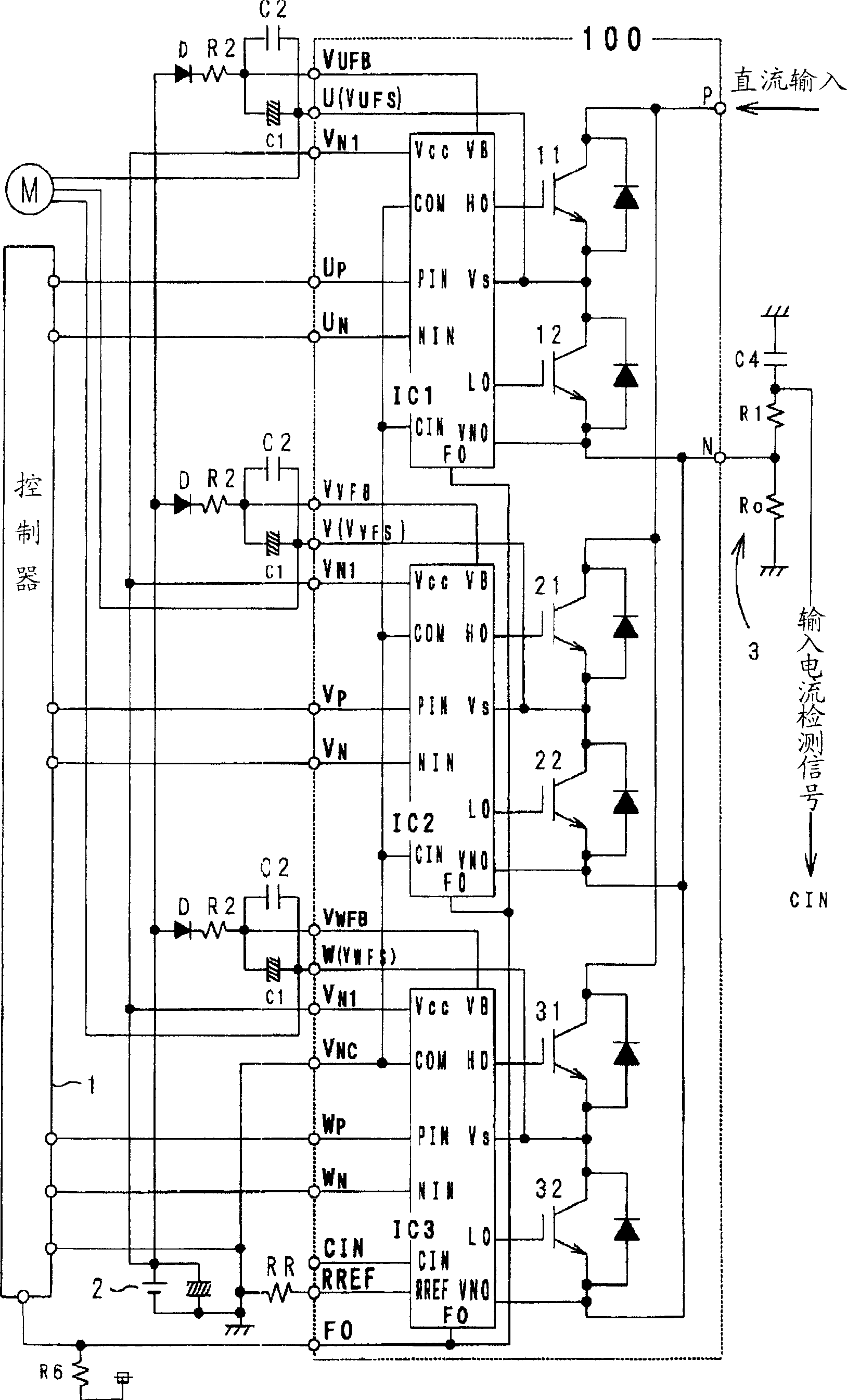
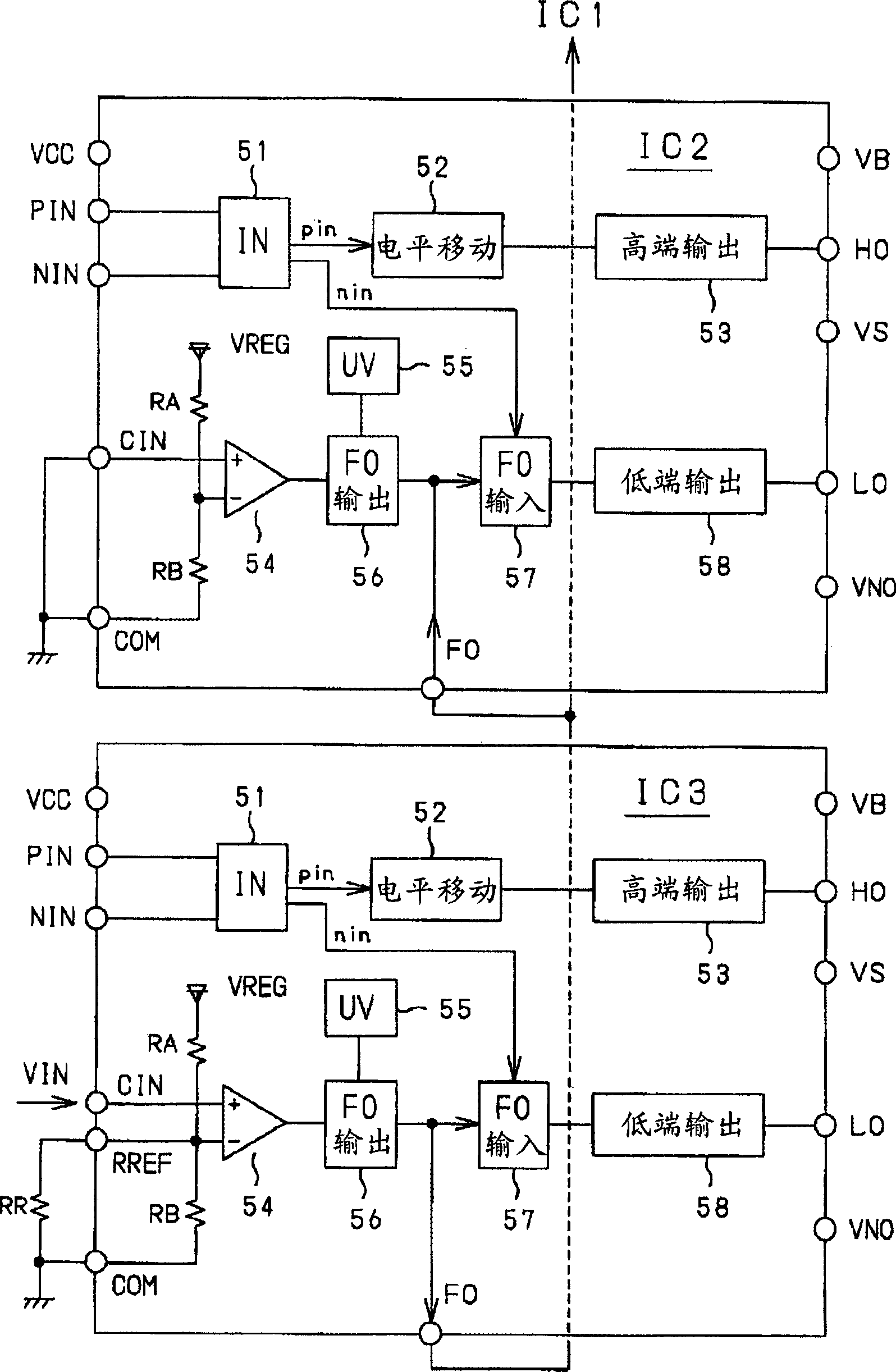
[0020] figure 1 A circuit diagram showing a power semiconductor device 100 including six IGBTs (11, 12, 21, 22, 31, 32) and three control integrated circuits (IC1-IC3) for switching and controlling these IGBTs. As a system, its It includes: a controller 1 for controlling the power semiconductor device 100 ; a power supply 2 for supplying power to the power semiconductor device 100 ; and an input current detection circuit 3 composed of a shunt resistor Ro, a resistor R1 , and a capacitor C4 . The control block diagram of IC2 and IC3 is in figure 2 Indicated.

[0021] exist figure 1 Among them, IGBTs (11, 12), (21, 22), and (31, 32), which are push-pull output circuit connections, are connected in parallel between the terminals P and N for supplying the DC input voltage to the power semiconductor device 100, respectively. In the same figure, corresponding to the actual configuration in the package, the IGBTs are arranged in a vertical column, and these 6 IGBTs are as Figur...

Embodiment approach 2

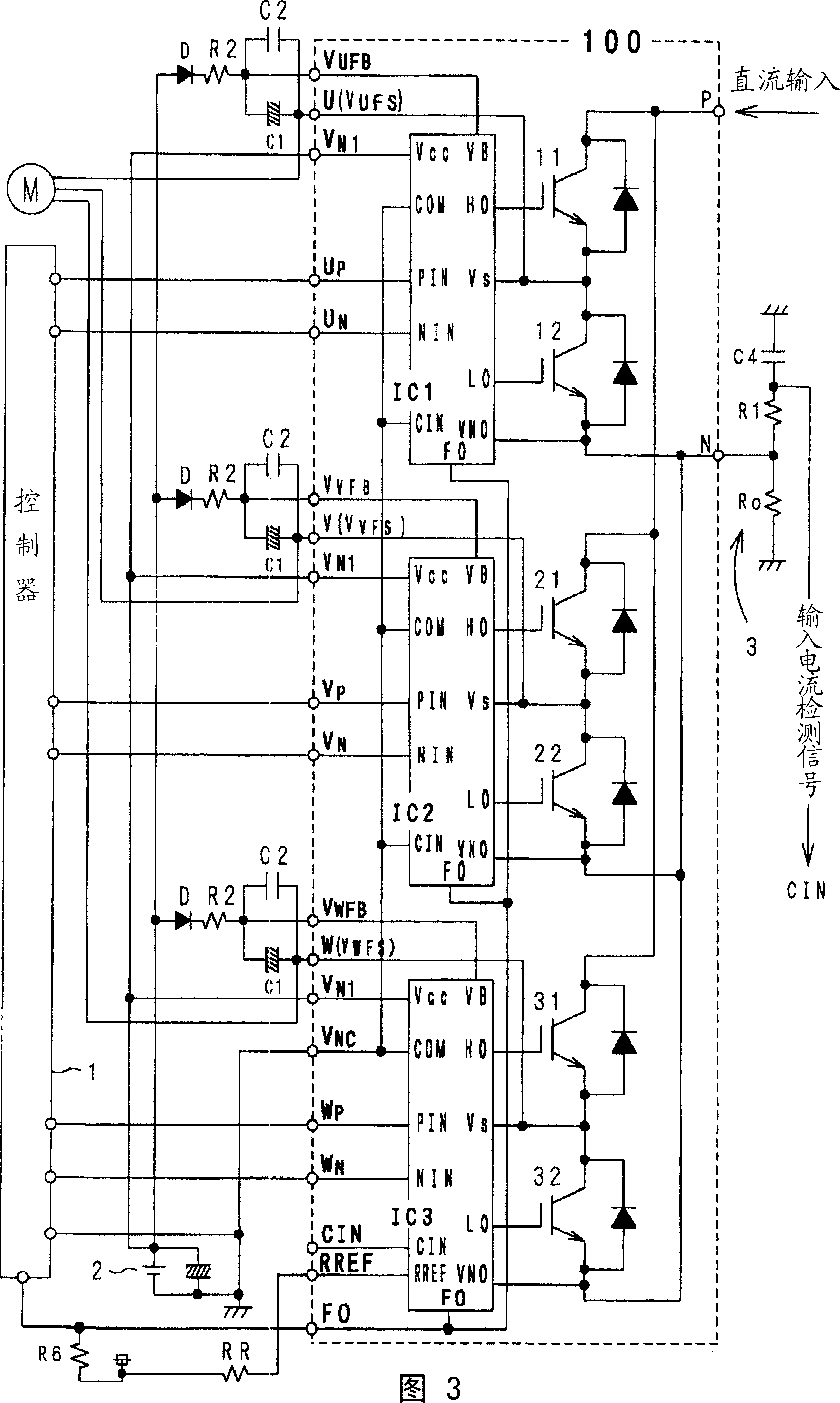
[0035] In Figure 3 and Figure 4Embodiment 2 of this invention is shown. exist figure 2 In this case, the resistance RR is connected in parallel with the resistance RB by grounding one end of the resistance RR, but in this Figure 4 , connect one end of the resistor RR to the internal reference potential. At this time, the resistor RR is connected in parallel with the resistor RA. With respect to the reference voltage to comparator 54 when no external resistor RR is connected, when Figure 4 When the external resistor RR is connected like this, the reference voltage will rise. Therefore, it is possible to increase the level of overcurrent protection tripping, and it is suitable for a design that focuses on improving the accuracy of overcurrent protection.

[0036] exist figure 2 Comparing IC3 and IC2 of the same type as in the past, it can be seen that in the present invention, only the terminal RREF for leading the reference input part of the comparator 54 to the outs...


PUM


Abstract

The object of the invenion is to provide a semiconductor device in which the level of overcurrent protection trip can be altered easily, without requiring significant revisions in the design. The semiconductor device comprises a plurality of power-switching semiconductor elements, a control integrated circuit for driving them, and a circuit performing overcurrent protection, by detecting the current flowing through the power-switching element, comparing the detection signal with a voltage obtained from a reference voltage and turning the power-switching element off when an overcurrent is detected. The semiconductor device further comprises a terminal (RREF) for leading out the line of the voltage obtained from a reference voltage and regulates the level of overcurrent protection trip, by connecting an external resistor (RR) between that terminal and the ground and regulating the voltage obtained from a reference voltage.

Description

technical field [0001] The present invention relates to a power semiconductor device including a power switching semiconductor element and a control integrated circuit for driving it. Background technique [0002] When the semiconductor device is a converter module with 3-phase output, it includes: 6 power switching semiconductor elements IGBT (Insulated Gate Bipolar Transistors) constituting a 3-phase bridge and IGBTs provided in each phase to drive these IGBTs. 3 control integrated circuits. In addition, in order to achieve the purpose of overcurrent protection, the current flowing through the IGBT of each phase is detected by a shunt resistor connected to the outside of the semiconductor device, and the voltage detected by the shunt resistor is taken into the above-mentioned control integrated circuit 1 of. In the comparator in the control integrated circuit, the reference voltage generated on the reference resistor is compared with the above-men...

Claims


Application Information

Patent Timeline
Patent Type & Authority Applications(China)
IPC IPC(8): H03F1/52H02M1/00H02M7/48H02M7/5387
CPCH02M1/32H03K17/6871H02M2001/0009H03K17/0828H02M2001/0025H03K17/567H02M1/0009H02M1/0025H03K19/00H03K19/01
Inventor 坂田浩司田中智典
Owner MITSUBISHI ELECTRIC CORP
Why Eureka
Try Eureka