
Printed circuit base plate

A technology for printed circuit substrates and electrical components, which is applied in the fields of printed circuit, printed circuit, printed circuit manufacturing, etc., and can solve problems such as poor connection of connecting pins, heightening of electric bridges, narrowing of intervals, etc.

Active Publication Date: 2010-08-25
SAMSUNG ELECTRONICS CO LTD
View PDF1 Cites 0 Cited by
  • Summary
  • Abstract
  • Description
  • Claims
  • Application Information

AI Technical Summary

Problems solved by technology

However, in the case of the lead-free solder from which the lead component is removed in this way, the fluidity in the molten state is relatively lower than that of the conventional solder containing the lead component, and the flow of the lead-free solder between the connection pin and the inner surface of the installation hole is relatively low. Not smooth, therefore, there is a risk of fixing and poor connection of the connecting pin
[0006] Therefore, in order to solve this problem, it is necessary to increase the diameter of the installation hole provided on the printed circuit board, but if the diameter of the installation hole is increased in this way, the interval between the adjacent installation holes becomes narrow, so there is a process of adding solder The problem that the possibility of a bridge between adjacent bosses in the middle becomes higher

Method used


Image

  • Printed circuit base plate
  • Printed circuit base plate
  • Printed circuit base plate

Examples


Embodiment approach

[0025] First, a first embodiment of the present invention will be described with reference to FIG. 1 .

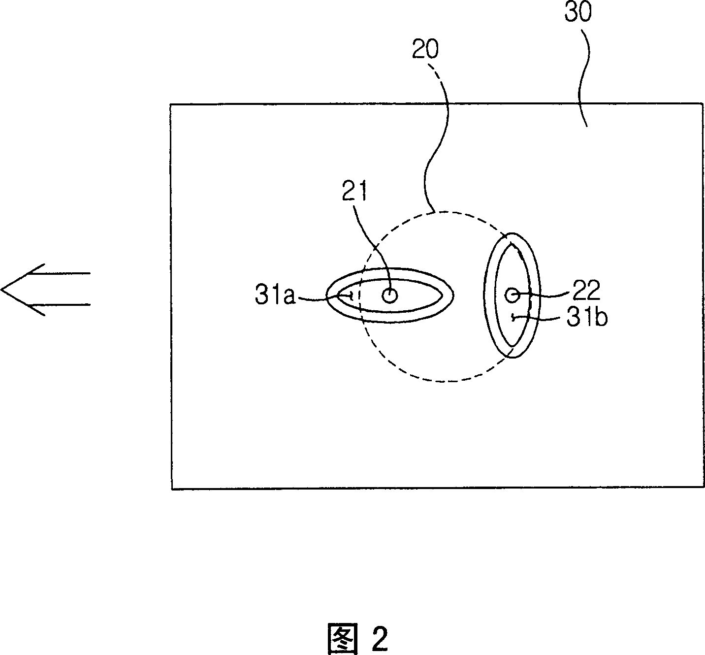
[0026] As shown in the figure, on the printed circuit board 10 in the present invention, a plurality of installation holes 11a, 11b that can install electrical components 20 such as ICs, capacitors, resistors, etc. are provided, and the adjacent parts of the installation holes 11a, 11b are provided. There are a plurality of lands 12 electrically connected to electrical components 20 by soldering with lead-free solder. At this time, at least a pair of connecting pins 21 and 22 that can be inserted through the installation holes 11a and 11b and can be connected by welding are provided on the electrical component. In this embodiment, a pair of connecting pins are provided in parallel on the electrical component 20 Pins 21, 22.

[0027] Therefore, after the connection pins 21, 22 of the electrical component 20 are inserted through the installation holes 11a, 11b of the printed...


PUM


Abstract

The invention provides a printed circuit board in which electric components are fixed and connected with lead-free solder from which lead components are removed. An electric component having a plurality of connection pins is installed, and there are formed a plurality of installation holes through which a plurality of connection pins are penetrated and fixed by soldering with lead-free solder. The installation holes are extended long in one direction, and formed to have short axes of predetermined lengths and long axes of relatively long lengths compared with the short axes. Consequently, intervals between the adjacent installation holes are maintained constant, and a space sufficient for the flow of the lead-free solder to both ends can be secured between the inner surface on the long axis side of the installation hole and the outer surface of the connection pin.

Description

technical field [0001] The present invention relates to a printed circuit board, and more specifically, to a printed circuit board to which lead-free solder from which lead components have been removed is applied. Background technique [0002] In general, printed circuit boards are built into various electronic products and are used to control the operation of electronic products. They are formed in a sheet shape and are provided with various electrical components such as ICs, capacitors, and resistors, and each electrical component interact to generate certain control signals. [0003] On such a printed circuit board, as disclosed in the following patent document 1, there are a plurality of installation holes in which various components can be installed, and the installation holes are provided adjacent to the installation holes around the installation holes, and connected to the circuit board. The parts are electrically connected to the boss, and the electrical part has a ...

Claims


Application Information

Patent Timeline
Patent Type & Authority Patents(China)
IPC IPC(8): H05K1/16H05K1/11H05K1/02
CPCH05K1/116H05K1/182H05K3/3405H05K3/3457H05K2201/0939
Inventor 金光烈
Owner SAMSUNG ELECTRONICS CO LTD
Learn More