
Eureka
For R&D, Eureka makes reading and utilizing patents & technical documents easy.
Eureka AIR
Designed for self-driven R&D workflows. Generate viable solutions, solve complex R&D challenges, empower your innovation with AI.

Eureka Materials
Designed for material experts only. Revolutionize your material R&D, from search, analyze, to developing new materials.

TechResearch
Generate reliable direction feasibility study reports for your R&D in just a few steps.

TechSeek
Discover and master advanced knowledge NOW. Basics, ideas, possibilities, all at once.

TechMind
As an expert in R&D Theories, TechMind can generates customized viable solutions instantly.

TechRisk
Analyze your overall solution with one click, know your potential R&D risks in advance.

TechMonitor
Get weekly tech updates, stay abreast of the latest tech innovations and key insights.
Substrate processing apparatus and substrate processing method
A substrate processing device and substrate technology, which is applied in the direction of photolithographic process exposure device, electrical components, semiconductor/solid-state device manufacturing, etc., can solve problems such as poor shape, poor exposure pattern size, and contamination of the lens of the exposure device.
- Summary
- Abstract
- Description
- Claims
- Application Information
AI Technical Summary
Problems solved by technology
Method used
Image

Examples
Embodiment Construction
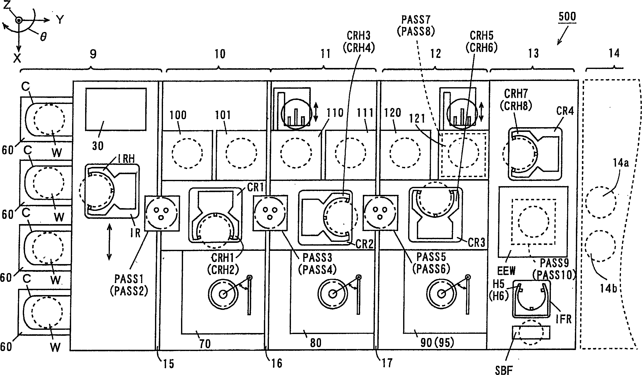
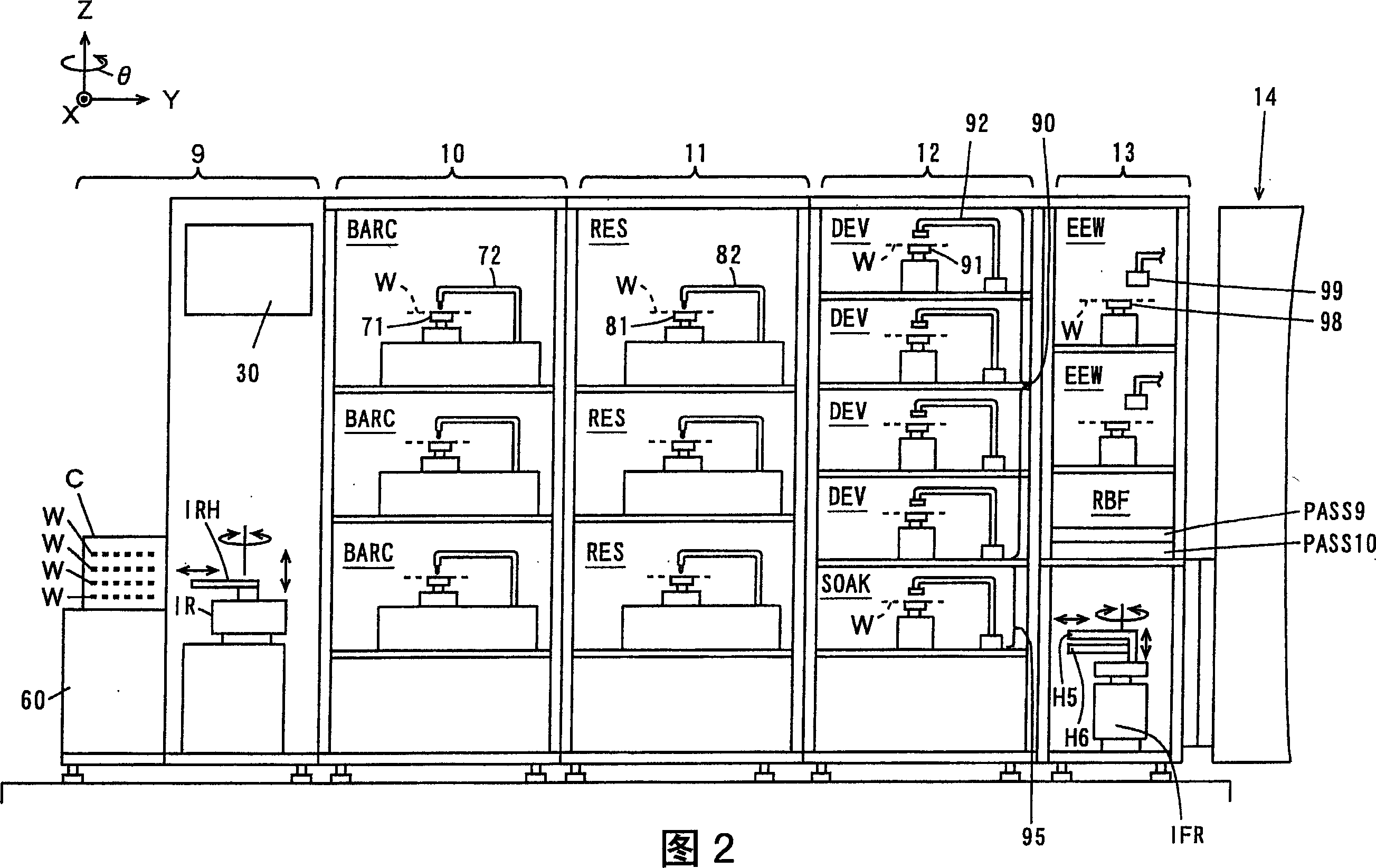
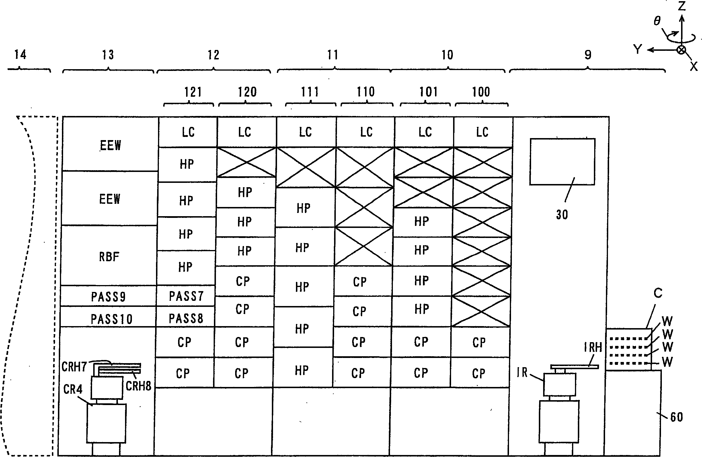
[0082] Next, a substrate processing apparatus according to an embodiment of the present invention will be described with reference to the drawings. In the following description, the term "substrate" refers to a semiconductor substrate, a substrate for a liquid crystal display device, a substrate for a plasma display, a glass substrate for a photomask, a substrate for an optical disk, a substrate for a magnetic disk, a substrate for a magneto-optical disk, a substrate for a photomask, etc. .
[0083] figure 1 It is a top view of a substrate processing apparatus according to an embodiment of the present invention.
[0084] exist figure 1 In each of the following drawings, in order to clarify the positional relationship, arrows are attached to indicate the X direction, the Y direction and the Z direction which are perpendicular to each other. The X direction and the Y direction are perpendicular to each other in the horizontal plane, and the Z direction corresponds to the vert...
PUM
 Abstract
Description
Claims
Application Information
 - R&D Engineer
- R&D Manager
- IP Professional
- Industry Leading Data Capabilities
- Powerful AI technology
- Patent DNA Extraction
Browse by: Latest US Patents, China's latest patents, Technical Efficacy Thesaurus, Application Domain, Technology Topic, Popular Technical Reports.
© 2024 PatSnap. All rights reserved.Legal|Privacy policy|Modern Slavery Act Transparency Statement|Sitemap|About US| Contact US: help@patsnap.com