Detection of silicon chip state in box and its center relocation method

A state detection and relocation technology, applied in the field of IC manufacturing, can solve the problems of space occupation, large number of sensors, and low relocation accuracy, and achieve the effect of high price, low cost, and simple debugging and maintenance

Inactive Publication Date: 2006-06-28
TSINGHUA UNIV
View PDF3 Cites 16 Cited by
  • Summary
  • Abstract
  • Description
  • Claims
  • Application Information

AI Technical Summary

Problems solved by technology

Compared with the pre-alignment of silicon wafers, the accuracy of relocation is relatively low. The detection and relocation of silicon wafers are

Method used


Image

  • Detection of silicon chip state in box and its center relocation method
  • Detection of silicon chip state in box and its center relocation method
  • Detection of silicon chip state in box and its center relocation method

Examples


Embodiment Construction

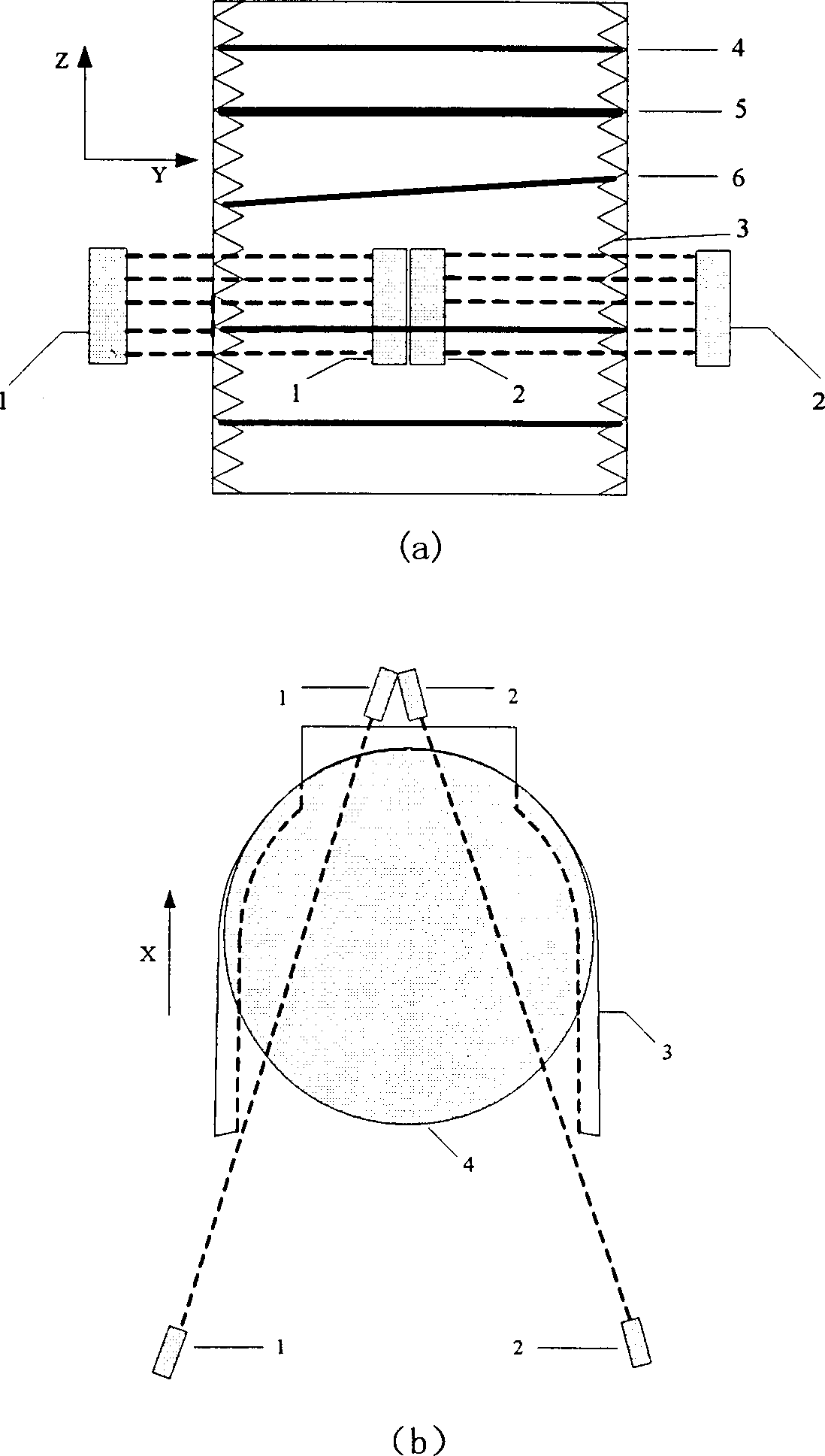
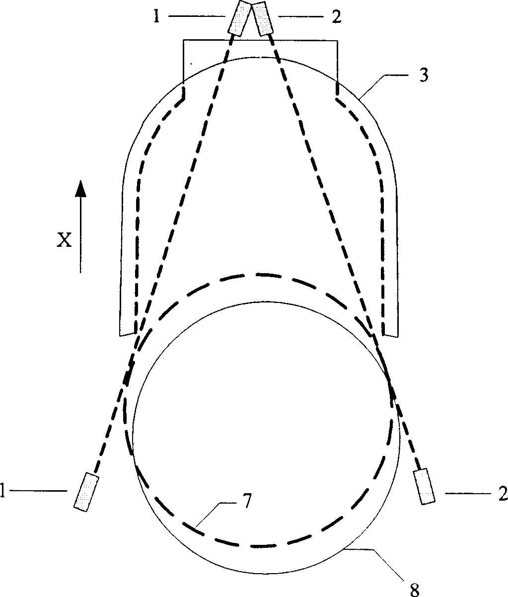
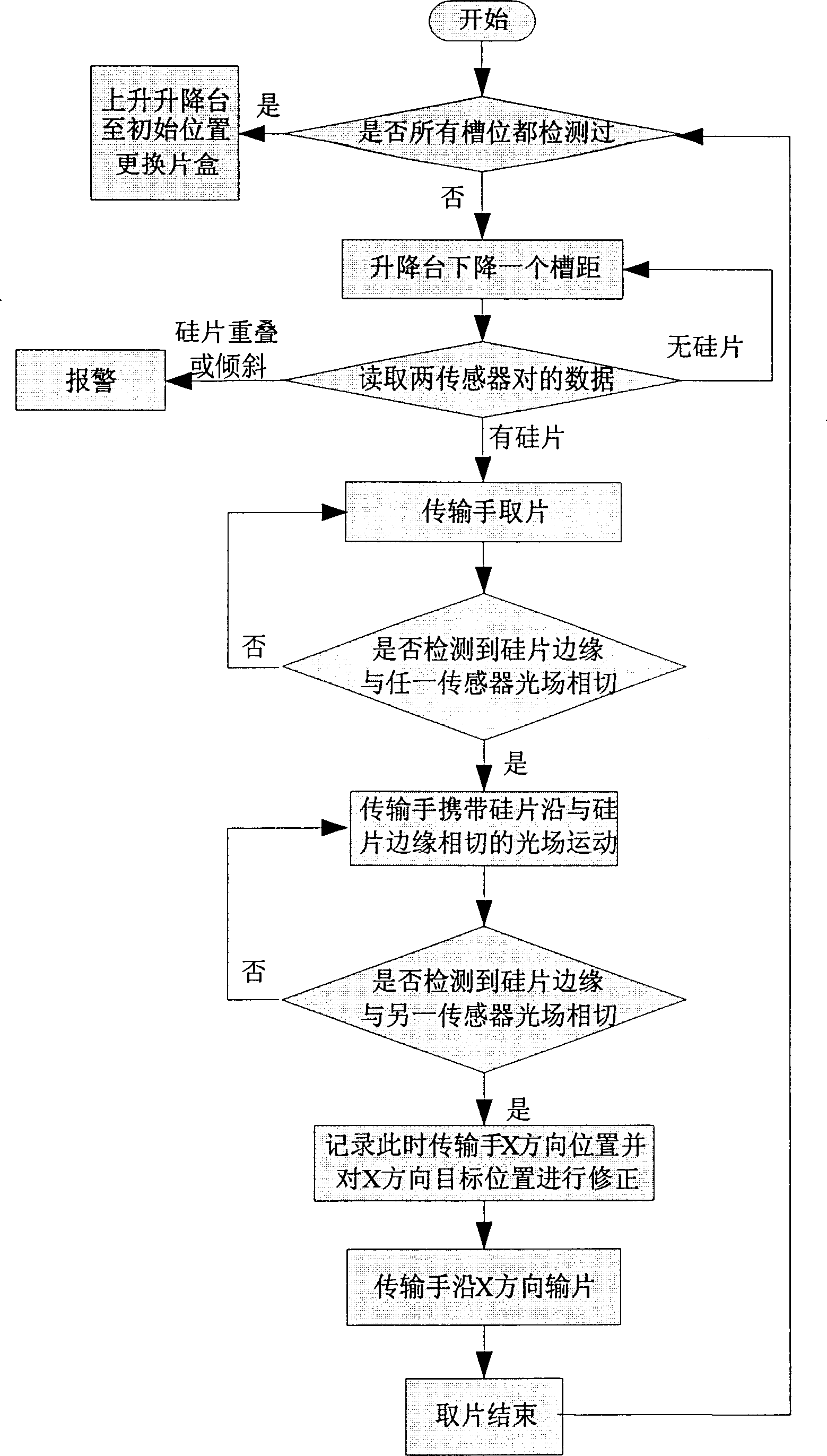
[0015] Silicon wafer detection and repositioning method of the present invention are described as follows in conjunction with embodiment and accompanying drawing:

[0016] The method for detecting the state of the silicon wafer in the cassette and its center repositioning method proposed by the present invention includes two parts: the detection of the state of the silicon wafer in the cassette and the repositioning of the silicon wafer during the transmission process by using two sets of transmission optical measuring elements;

[0017] Said transmissive optical measuring element is a sensor pair composed of a light-emitting element that emits a strip of light and a receiving element that receives the light emitted by the light-emitting element, wherein the light-emitting element emits a strip of light (when the object is in the strip light field When the light intensity received by the receiving element is weakened, the light-shielding area of ​​the object can be judged); the...


PUM


Abstract

This invention relates to a method for testing a silicon chip state in a box and re-location of its center, in which, the test method includes: designing a light intensity threshold value 10,11, testing the light intensity of any pair of sensors timely of 1S1, if 1S1=!0, then there is no silicon chip, when 10 > 1S1 >11, then there is one, when 1S1 is smaller or equals to 11, there are laminated silicon chips, if the two sensors have different light shading time, then the chips are at the tilted state, the method for re-locating the center includes: when the edges of the chips are tangential to the light-fields of the two sensors at the same time, then the position of a transport mechanical hand on the X direction is P0, when the edges of the chips are tangential to the light-fields of the two sensors, then its position is P1, if P1= P0, then the chips are at the ideal position, if not, the difference between them is the distance should be compensated on the X direction.

Description

technical field [0001] The invention belongs to the technical field of IC manufacturing, in particular to a method for detecting and relocating the state of a silicon wafer. Background technique [0002] Silicon wafer detection and repositioning are important components of the wafer transport system of IC manufacturing equipment such as lithography machines. Silicon wafer detection needs to detect whether there are silicon wafers in the corresponding slot and whether their position is normal before the transfer hand picks up the wafers, and find out that the silicon wafers are overlapped, silicon wafers are tilted and other state errors, so that the transfer hand can take the wafers correctly. The repositioning of the center of the silicon wafer has two main functions: 1. Make the silicon wafers be accurately fed into the cassette, and correct the deviation of the wafer center during the unloading process; 2. Roughly locate the center of the silicon wafer taken out of the ca...

Claims


Application Information

Patent Timeline
IPC IPC(8): H01L21/68G01B11/00G03F7/20
Inventor 宋亦旭赵雁南杨泽红王家钦李世昌贾培发邓志东
Owner TSINGHUA UNIV
Why Eureka
Try Eureka