Supercharge Your Innovation With Domain-Expert AI Agents!

Structure and method for failure analysis in a semiconductor device

A failure analysis and semiconductor technology, applied in semiconductor devices, semiconductor/solid-state device components, semiconductor/solid-state device testing/measurement, etc., can solve problems such as development lag

Active Publication Date: 2006-07-19
SAMSUNG ELECTRONICS CO LTD
View PDF1 Cites 14 Cited by
  • Summary
  • Abstract
  • Description
  • Claims
  • Application Information

AI Technical Summary

Problems solved by technology

Therefore, the lack of determination of the cause of failure can cause development delays

Method used


Image

  • Structure and method for failure analysis in a semiconductor device
  • Structure and method for failure analysis in a semiconductor device
  • Structure and method for failure analysis in a semiconductor device

Examples


Embodiment Construction

[0065] Preferred embodiments of the present invention will now be described in more detail below with reference to the accompanying drawings. However, this invention may be embodied in many different forms and should not be construed as limited to the embodiments set forth herein. Rather, these embodiments are provided so that this disclosure will be thorough and complete.

[0066] In the drawings, the thicknesses of layers and regions are exaggerated for clarity. It will be understood that when a layer is referred to as being "on" another layer or substrate, it can be directly on the other layer or substrate, or intervening layers may also be present. Throughout the specification, like reference numerals are used to refer to like elements.

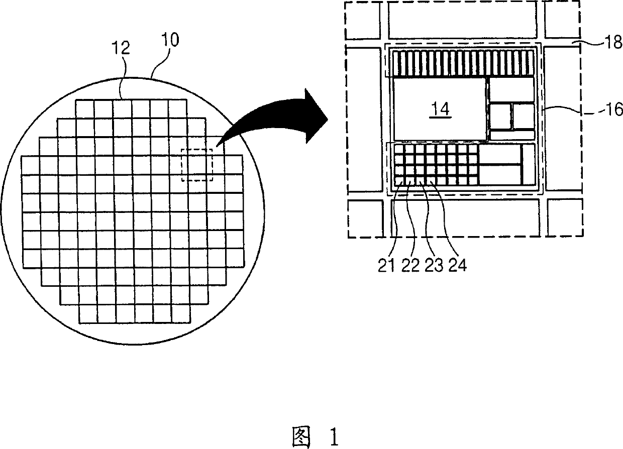
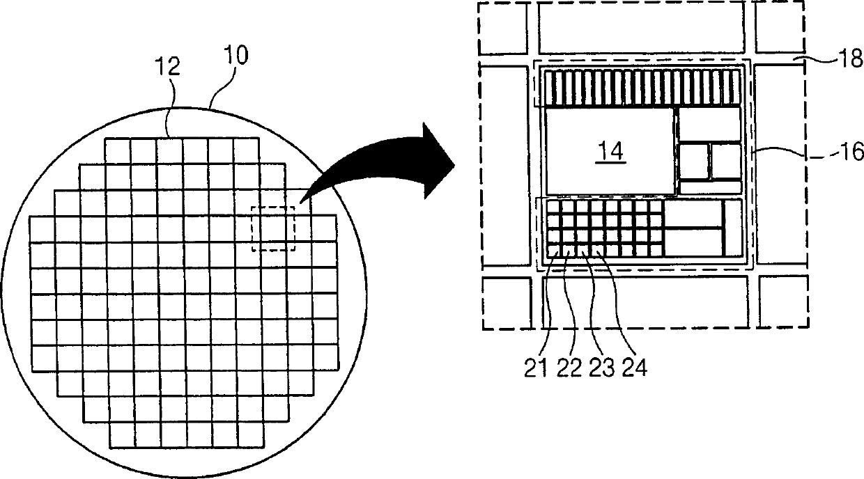
[0067] FIG. 1 is a plan view showing an analysis structure according to the present invention.

[0068] Referring to FIG. 1 , a plurality of die 12 including a product area 14 and an auxiliary area 16 are disposed on a semiconductor wa...


PUM


Abstract

The invention discloses an analysis structure and method for semiconductor failure analysis. The structure includes: a plurality of analysis fields arranged on a predetermined area of ​​a semiconductor device; semiconductor transistors arranged in each of the analysis fields, the semiconductor transistors arranged in an array; word lines arranged in the plurality of on each of the analysis fields, connecting the semiconductor transistors to each other in a first direction; and a bit line structure, on each of the plurality of analysis fields, connecting the semiconductor transistors to each other in a second direction, wherein, The bit line structures are configured in different patterns in each of the plurality of analysis fields.

Description

technical field [0001] The present invention relates to failure analysis of semiconductor devices, and more particularly, to structures and methods for failure analysis. Background technique [0002] For mass production of semiconductor devices, reliable process technologies that can provide profitable yields are desired. A process for improving reliability and stability of process technology includes the steps of designing a semiconductor device, manufacturing a sample of the semiconductor device, and testing the sample. Failure analysis of semiconductor devices is a feedback process that involves finding and correcting the root cause of defects to overcome the problems created by the defects. [0003] Strategies for designing and manufacturing semiconductor devices can be highly integrated with failure analysis results. Therefore proper failure analysis is critical to improve the quality of semiconductor devices. Incorrect failure analysis can lengthen the period requir...

Claims


Application Information

Patent Timeline
Patent Type & Authority Applications(China)
IPC IPC(8): H01L23/544H01L21/66
CPCG01R31/2884G11C5/06G11C7/18
Inventor 李起岩权相德李钟弦
Owner SAMSUNG ELECTRONICS CO LTD
Features
  • R&D
  • Intellectual Property
  • Life Sciences
  • Materials
  • Tech Scout
  • Unparalleled Data Quality
  • Higher Quality Content
  • 60% Fewer Hallucinations
Learn More