Touch control plate with finger print identifying function and its manufacturing method

A manufacturing method and technology of a touch panel, applied to instruments, computer parts, graphics reading, etc., can solve problems that cannot be effectively solved, solvent pollution, spherical interstitial particles of different sizes, etc., to achieve market competition, Improvement of industrial competitiveness and cost-effective effect

Active Publication Date: 2006-08-09
AU OPTRONICS CORP
View PDF0 Cites 5 Cited by
  • Summary
  • Abstract
  • Description
  • Claims
  • Application Information

AI Technical Summary

Problems solved by technology

[0013] Moreover, because the touch panel 20 can be made of light-transmitting materials and applied to the surface of a display panel, a screen or a tablet computer, once the flatness of the touch panel 20 is lowered, it will greatly affect the display quality of the display panel or screen. , this is because the light from the display panel or screen needs to pass through the touch panel 20 before entering the user's line of sight, so the conductive elastic film layer 28 will affect the flatness and uniformity of the image
[0014] In this way, the disadvantage of insufficient support of the conductive elastic film layer 28 not only affects the length of the product life of the touch panel itself, but also affects the quality of displayed images for electronic products (such as display panels or screens) using the touch panel. quality
[0015] In the prior art, although there is an initial solution mixed with spherical spacers 14 (spacers), which is spread on the transistor plate 21 in the form of spin-on coating, and then the solution is dried, so that the spherical spacers 14 (spacer) is dispersed throughout the transistor board 21, and is coated on the edge of the outer frame with a partition frame glue 29, although it can slightly improve the problem of insufficient support in the middle part of the conductive elastic film layer 28
However, the following problems are still caused: 1) the solvent will pollute and corrode the components of the transistor plate 21, so that when the user touches the pressure, the sensitivity of signal discrimination is reduced
2) The spin-coating distribution method will cause uneven dispersion of spherical spacers, and the size of spherical spacer particles may be different, thereby affecting the smoothness of the conductive elastic film layer 28
It makes it easy to identify some positions, but difficult or impossible to identify some positions
Therefore, this method cannot effectively solve the above-mentioned existing problems

Method used


Image

  • Touch control plate with finger print identifying function and its manufacturing method
  • Touch control plate with finger print identifying function and its manufacturing method
  • Touch control plate with finger print identifying function and its manufacturing method

Examples


Embodiment Construction

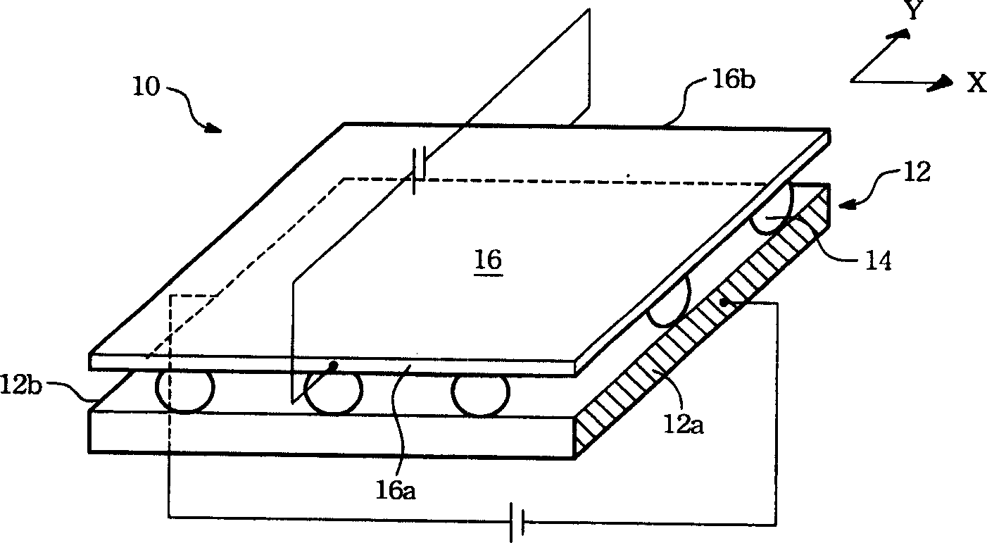
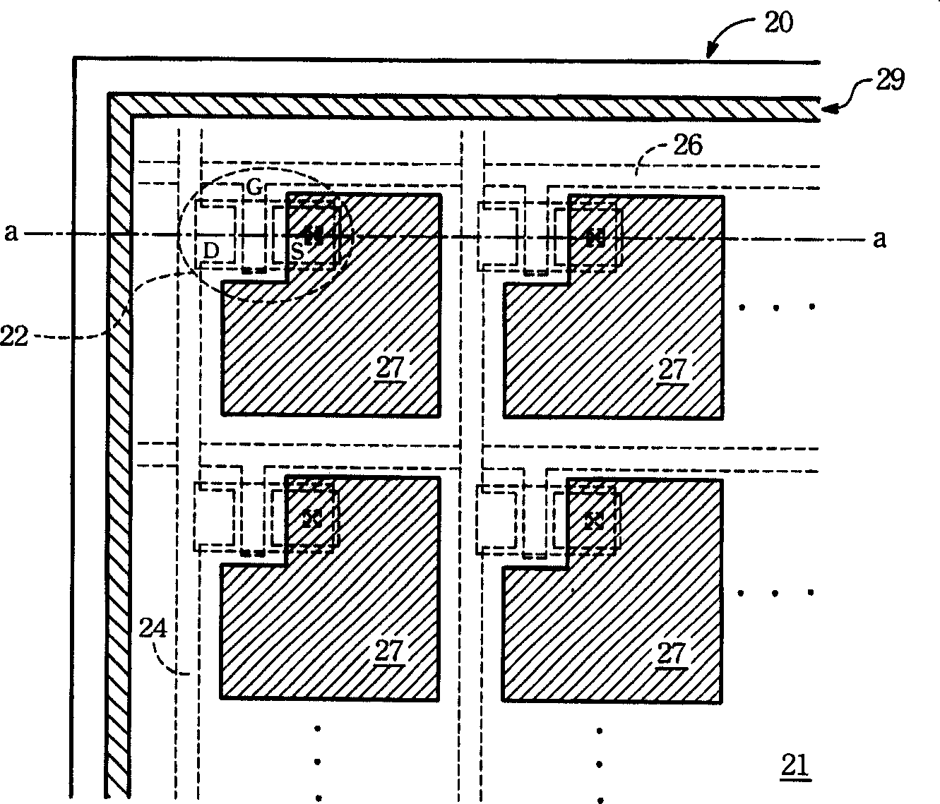
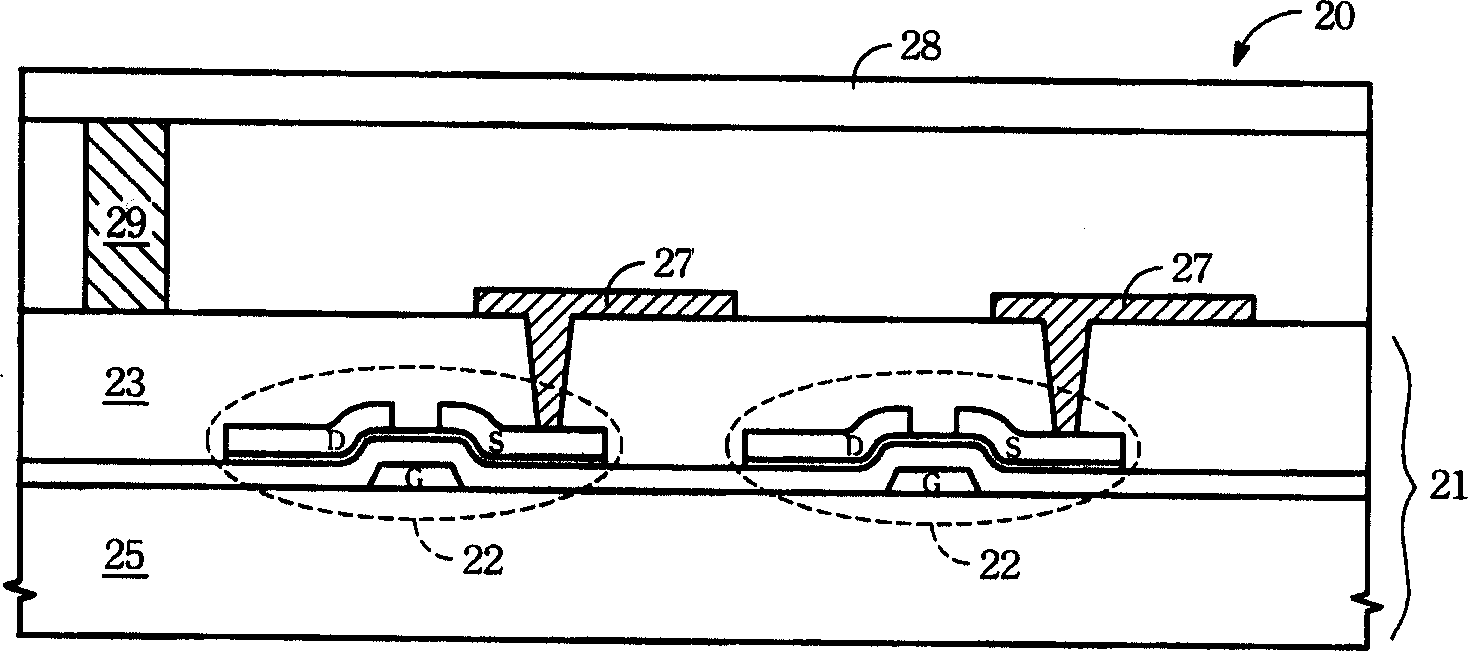
[0055] Please refer to Figure 3A , Figure 3B , which is a three-dimensional exploded view and a cross-sectional view of a part of the touch panel 40 with fingerprint recognition function of the present invention; Figure 3B is corresponding to Figure 3A The a-a section line in . Figure 3A Only a part of the touch panel 40 is shown, and only four thin film transistors 42 are shown as representatives. Although this embodiment uses the bottom gate thin film transistor 42 (Bottom Gate TFT) as a template, the top gate thin film transistor ( Top Gate TFT) can also be used. The touch panel 40 provided by the present invention can be applied to an electronic device, such as a tablet computer, a display panel or a screen, and the like. The touch panel 40 includes a transistor panel 41 , a plurality of conductive blocks 47 , a support pattern layer 52 and a conductive elastic film layer 48 .

[0056] The transistor board 41 includes a substrate 45 , thin film transistors 42 arr...


PUM


Abstract

Being applicable to electronic equipment, the touch pad includes a transistor plate, multiple conduction region blocks, a support pattern layer and a conductive elastic membrane layer. Array of thin film transistor is arranged on the transistor plate. Being formed on the transistor plate, multiple conduction region blocks are electrically connected to each thin film transistor respectively. Being formed on the transistor plate, the support pattern layer includes multiple openings in order to expose part of each conduction region block and / or transistor plate. The conductive elastic membrane layer is placed on the support pattern layer.

Description

technical field [0001] The invention relates to a touch panel with a fingerprint recognition function, in particular to a touch panel with a new supporting structure. Background technique [0002] With the advancement of technology, the input devices of electronic products are becoming more and more diversified. Among the many input devices, besides the most familiar keyboard and mouse, the touch panel input device is becoming more and more common. The touch panel with fingerprint identification function has been used in identification devices or other similar electronic devices, and is usually used by research units or high-tech companies to be used at the entrances and exits of buildings or laboratories. Identify the identities of those entering and exiting. Recently, the touchpad is integrated with the display to produce a tablet computer with touch input to the screen, which not only saves the space that the input device must occupy, but also allows the user to directl...

Claims


Application Information

Patent Timeline
Patent Type & Authority Applications(China)
IPC IPC(8): G06K11/06
Inventor 翁健森
Owner AU OPTRONICS CORP
Why Eureka
Try Eureka