Semiconductor device and its manufacturing method
A manufacturing method and semiconductor technology, applied in the direction of semiconductor/solid-state device manufacturing, semiconductor devices, electrical components, etc., can solve problems such as inability to meet requirements, and achieve the effect of high withstand voltage
- Summary
- Abstract
- Description
- Claims
- Application Information
AI Technical Summary
Problems solved by technology
Method used
Image

Examples
Embodiment Construction
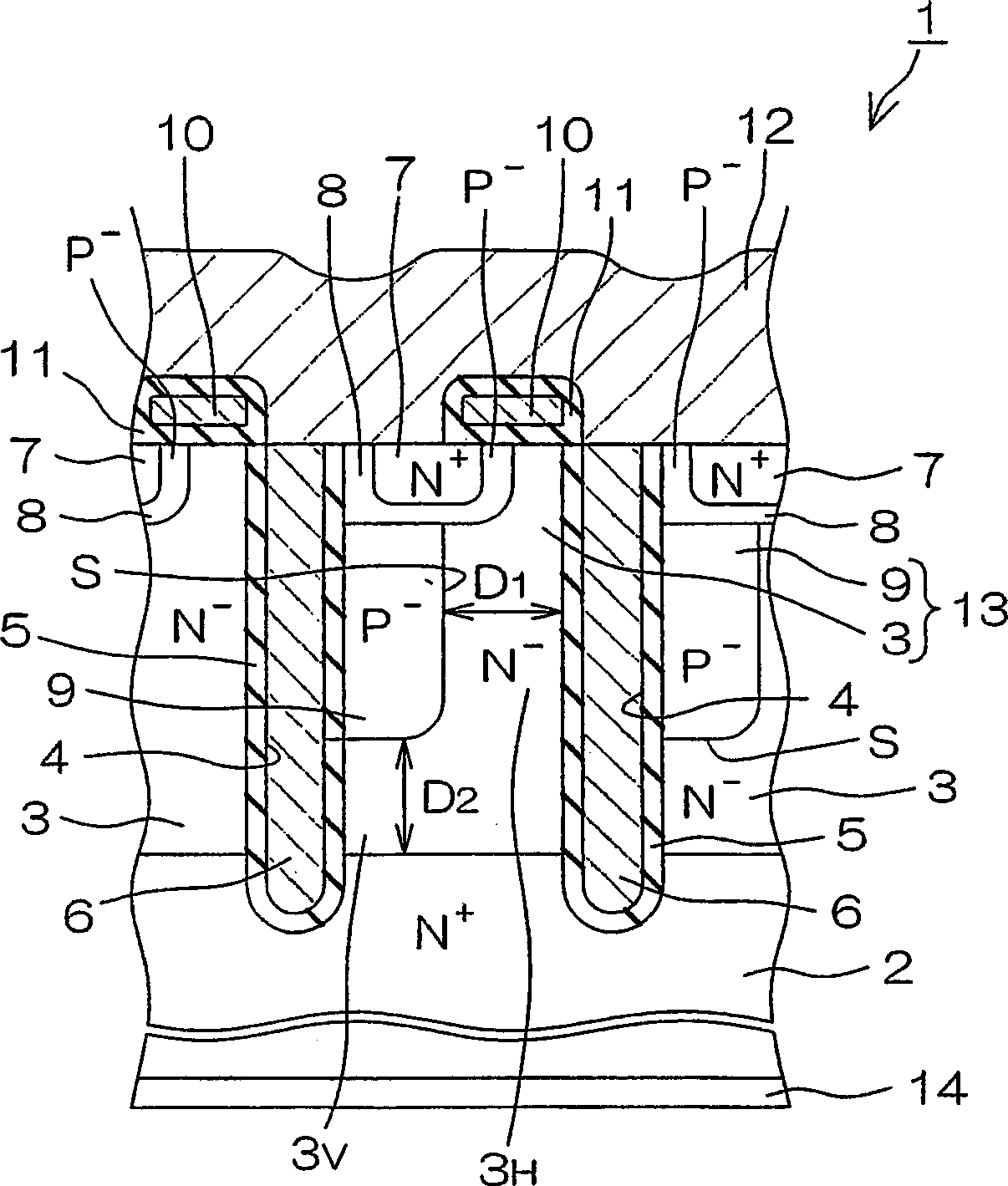
[0047] figure 1 It is a schematic cross-sectional view showing the structure of the semiconductor device 1 according to the first embodiment of the present invention.
[0048] In the constituent conductivity type is N + On the silicon substrate 2 constituting the drain region, a semiconductor layer 13 forming a so-called super junction structure is provided. The semiconductor layer 13 includes conductivity type N - type of the drift layer 3 and the conductivity type is P - type RESURF layer 9, the drift layer 3 and the RESURF layer 9 are arranged so that they appear alternately (repeatedly) in sequence on the silicon substrate 2 in parallel and laterally.
[0049] A plurality of trenches 4 penetrating the semiconductor layer 13 to a depth of the silicon substrate 2 are formed substantially parallel to each other. The trench 4 has an inner side wall that is substantially perpendicular to the silicon substrate 2, and is perpendicular to the figure 1 Extend in the directio...
PUM
 Abstract
Description
Claims
Application Information
 - Generate Ideas
- Intellectual Property
- Life Sciences
- Materials
- Tech Scout
- Unparalleled Data Quality
- Higher Quality Content
- 60% Fewer Hallucinations
Browse by: Latest US Patents, China's latest patents, Technical Efficacy Thesaurus, Application Domain, Technology Topic, Popular Technical Reports.
© 2025 PatSnap. All rights reserved.Legal|Privacy policy|Modern Slavery Act Transparency Statement|Sitemap|About US| Contact US: help@patsnap.com