

A printed circuit board and production method thereof
A printed circuit board and circuit board technology, which is applied in the fields of printed circuit manufacturing, multi-layer circuit manufacturing, printed circuit, etc., can solve the problems of high cost and limitation, and achieve the effects of convenience, shortening the manufacturing cycle, and ensuring the quality of production
- Summary
- Abstract
- Description
- Claims
- Application Information
AI Technical Summary
Problems solved by technology
Method used
Image

Examples
Embodiment Construction
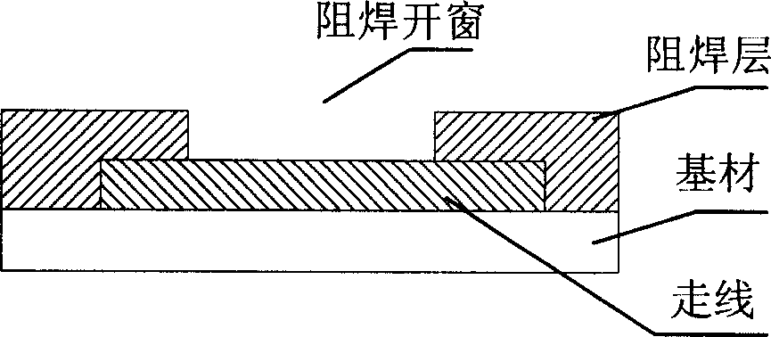
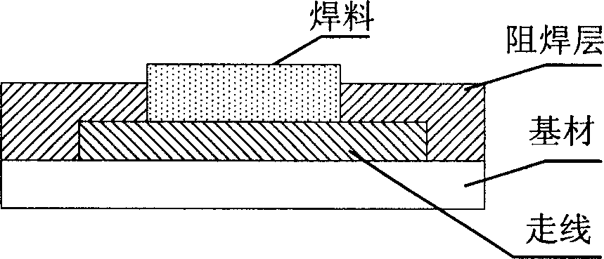
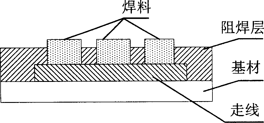
[0028] The structure of the PCB board of the present invention is as figure 1 As shown, in PCB design, for PCB traces that need to carry high current, design a solder mask window with a certain width above the trace, and then fill the solder mask window with solder when assembling devices on the PCB. When the solder melts and electrically bonds with the trace, as figure 2 As shown, it is equivalent to increasing the cross-sectional area of the wiring and improving the current carrying capacity of the wiring. According to the requirements of PCB structure, characteristics of solder and welding process, etc., the design of solder mask opening has the following characteristics:
[0029] 1. The shape and number of solder mask openings are not limited, and are determined by the number and shape of the traces carrying high current on the PCB;
[0030] 2. The direction of the solder mask opening is consistent with the direction of the trace, and it is distributed continuously al...
PUM
 Abstract
Description
Claims
Application Information