Chip general detector and its structure method

A general-purpose testing and chip technology, applied in measuring devices, electronic circuit testing, single semiconductor device testing, etc., to avoid repeated development, reduce difficulty, save time and cost

Inactive Publication Date: 2006-11-08
HISILICON TECH
View PDF0 Cites 33 Cited by
  • Summary
  • Abstract
  • Description
  • Claims
  • Application Information

AI Technical Summary

Problems solved by technology

[0012] The purpose of the present invention is to overcome the defects in the above-mentioned existing single test platform mother-daughter board technical scheme, propose a kind

Method used


Image

  • Chip general detector and its structure method
  • Chip general detector and its structure method
  • Chip general detector and its structure method

Examples


Embodiment

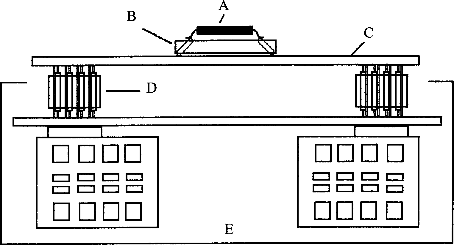
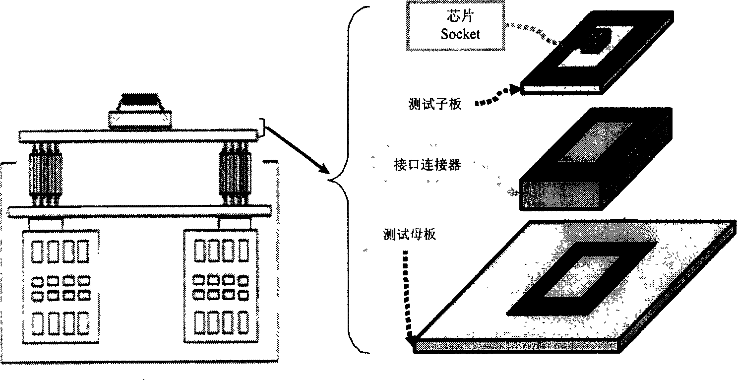
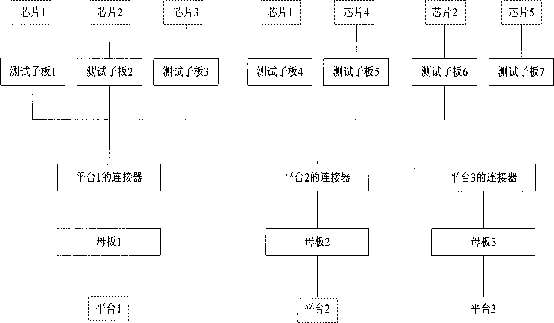
[0064] like Image 6 As shown, the universal interface connector 2 includes 16 digital interface modules 21, respectively denoted by "DIGxx", 2 analog interface modules 22, respectively denoted by "ANAxx", and 4 power interface modules 23, respectively denoted by "DPSxx" express. The digital interface module 21 , the analog interface module 22 and the power interface module 23 have fixed positions, and the fixed positions are determined by the unified interface standard defined in this embodiment. In this way, the universal interface connector 2 can connect the digital signals, analog signals and power signals on the channels of the test daughter board 3 and the test motherboard 1 respectively.

[0065] In this embodiment, the universal interface connector 2 further includes four control switch interface modules 24, which are denoted by "UTIxx". The control switch interface modules 24 have fixed positions matching the unified interface standard and are used for connecting to ...


PUM


Abstract

This inventioin discloses a general test device for chips including a test mother board, a test sub-board and a general interface connector, in which, the mother board is corresponding to a test platform exclusively and connected with one end of the connector, the sub-board is corresponding to a chip structure and connected with the other end of the connector, which applies a standard interface. This invention also discloses a method for structuring the general test device for chips, which designs the general interface connector in light of designed uniform interface standard and sets up associations between interface signals of the boards and the connector, which realizes that a same test sub-board platform is used in different test mother boards and a same mother board uses different sub-boards.

Description

technical field [0001] The invention relates to semiconductor device testing technology, in particular to a chip universal testing device and a construction method thereof. Background technique [0002] In order to ensure the quality of semiconductor chips and reduce development costs, tests are generally performed on automatic test equipment (Automatic Test Equipment, abbreviated as ATE, referred to as testing machine) in the early stage of chip development. figure 1 As shown, it includes: Socket or HandlerContactor B, used to fix the packaged chip (Device Under Test, DUT) A to be tested; Device Interface Board (DIB) C; Test platform E. like figure 1 As shown, the DUT is connected to the DIB through the Socket, and the DIB is connected to the connection channel of the test platform through the pogo pin D. In this way, the test platform can transmit various signals to the various pins of the DUT through the wiring on the DIB. [0003] Alternatively, the testing device in...

Claims


Application Information

Patent Timeline
IPC IPC(8): G01R1/02G01R1/06G01R31/00G01R31/26G01R31/28H01L21/66
Inventor 张欣杨文进李益欢王宇林建军戈文李春雷
Owner HISILICON TECH
Why Eureka
Try Eureka