

Shielded electronic circuit unit and method of manufacturing the same
A technology of electronic circuit and manufacturing method, which is applied in the direction of printed circuit manufacturing, multilayer circuit manufacturing, circuit, etc., can solve the problems of insufficient electric shielding, unreliable adhesion, insufficient circulation of electroplating solution, etc., and achieve good electric shielding, connection Reliable condition, good cycle results
- Summary
- Abstract
- Description
- Claims
- Application Information
AI Technical Summary
Problems solved by technology
Method used
Image

Examples
Embodiment Construction
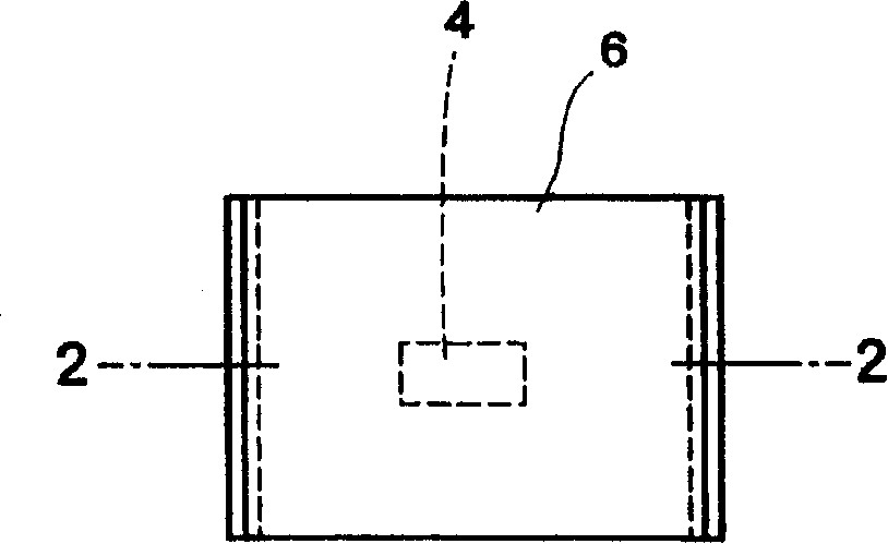
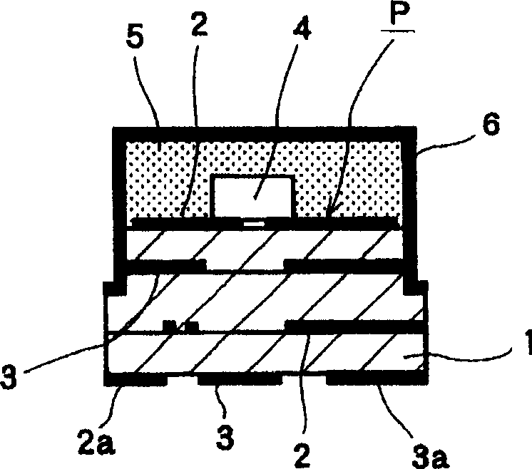
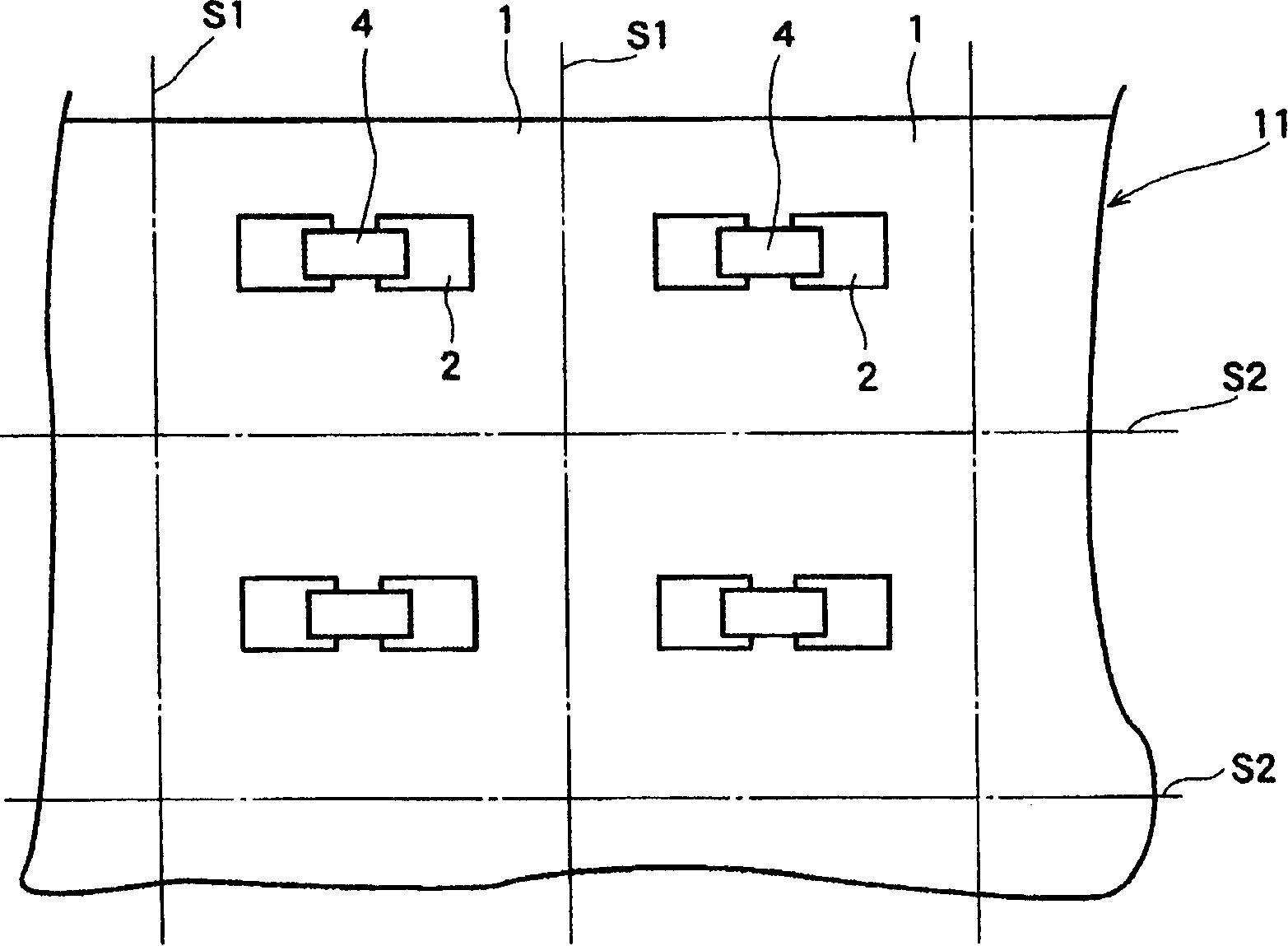
[0099] The accompanying drawings illustrating the electronic circuit unit of the present invention and its manufacturing method, figure 1 is a top view of the first embodiment of the electronic circuit unit of the present invention, figure 2 Yes figure 1 A cross-sectional view of the 2-2 line, image 3 It is a plan view showing the first step of the manufacturing method of the first embodiment of the electronic circuit unit of the present invention, Figure 4 is a sectional view showing the first step of the manufacturing method of the first embodiment of the electronic circuit unit of the present invention, Figure 5 It is a sectional view showing the second step of the manufacturing method of the first embodiment of the electronic circuit unit of the present invention, Image 6 It is a plan view showing the third step of the manufacturing method of the first embodiment of the electronic circuit unit of the present invention, Figure 7 is a sectional view showing the t...
PUM
 Abstract
Description
Claims
Application Information