Solid-state image sensor and image camera

A technology for solid-state imaging devices and semiconductors, which is applied in the fields of electrical solid-state devices, semiconductor devices, and semiconductor/solid-state device manufacturing, and can solve problems such as image quality degradation, difficulty in light convergence, and decreased sensitivity.

Inactive Publication Date: 2010-07-21
PANASONIC CORP
View PDF5 Cites 0 Cited by
  • Summary
  • Abstract
  • Description
  • Claims
  • Application Information

AI Technical Summary

Problems solved by technology

Then, in order to compensate for the reduction in light concentration efficiency caused by the miniaturization of the light receiving unit, when the light concentration of the microlens 23 is optimized in the wide opening 20A, it is difficult for a part of the incident light 24 to enter the narrow opening. Therefore, the incident light 24 passing through the opening 20B is reduced, and the sensitivity of the light receiving unit B receiving high-brightness light is greatly reduced.
And, in the peripheral portion of the solid-state imaging device, the incident angle of the incident light 24 is larger than that of the central portion, so the light transmitted through the opening 20B is more difficult to converge. The sensitivity of the light-receiving unit B of the above-mentioned is greatly reduced, resulting in sensitivity shading and color unevenness, so the quality of the obtained image is significantly degraded

Method used


Image

  • Solid-state image sensor and image camera
  • Solid-state image sensor and image camera
  • Solid-state image sensor and image camera

Examples


Embodiment approach 1

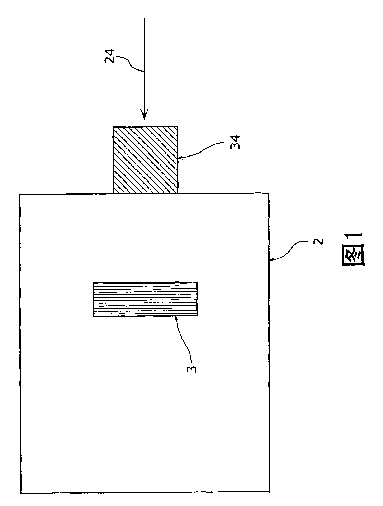
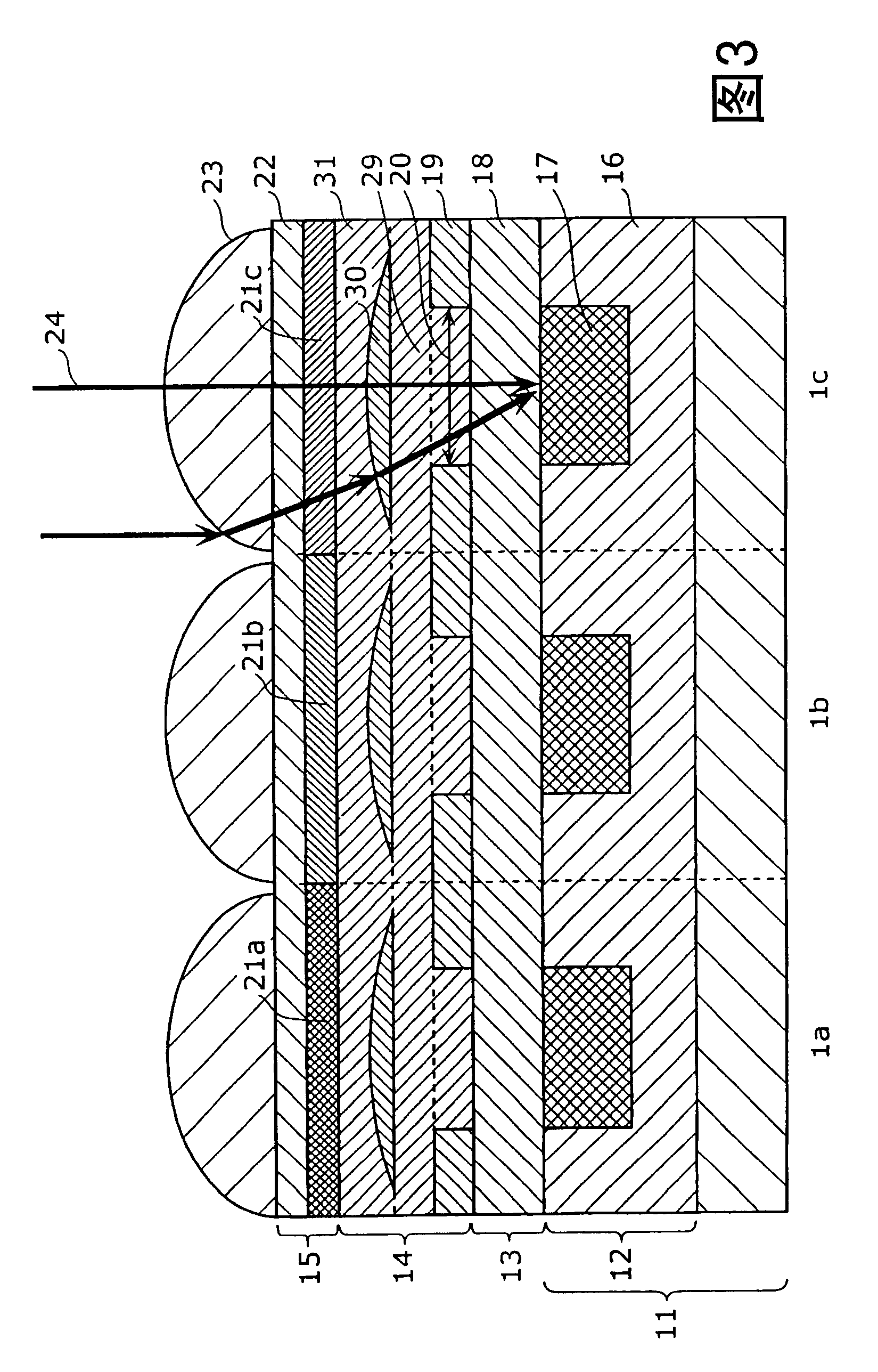
[0130] 8 is a cross-sectional view of light receiving units 111a, 111b, and 111c of the solid-state imaging device according to Embodiment 1 of the present invention. The semiconductor substrate 11, photoelectric conversion layer 12, and insulating layer 13 of each light receiving unit have the same structure as that of the conventional light receiving unit shown in FIG. 3 .

[0131] The metal layer 114 is a layer including the light-shielding film 19 and the in-layer lens 30 as in the conventional solid-state imaging device, but in the solid-state imaging device according to Embodiment 1 of the present invention, the metal layer 114 is embedded in the Form the opening 20 of the light-shielding film 19 in the same way as the high-refractive-index layer 125 made of a high-refractive-index material. The inner lens 30 has an interlayer film 31 formed on the inner lens 30 . Also, the color filter layer 15 including the interlayer film 22 is formed on the metal layer 114 , and the...

Embodiment approach 2

[0151] 11 is a cross-sectional view of light receiving units 211a, 211b, and 211c of the solid-state imaging device according to Embodiment 2 of the present invention. The semiconductor substrate 11, photoelectric conversion layer 12, and insulating layer 13 of each light receiving unit have the same structure as that of the conventional light receiving unit shown in FIG. 3 .

[0152] The metal layer 214 is a layer including the light shielding film 19 as in conventional solid-state imaging devices. However, in the solid-state imaging device according to Embodiment 2 of the present invention, the metal layer 214 has a high-refractive index layer 225 formed to fill the opening 20 of the light-shielding film 19 after forming the light-shielding film 19 . Constructed of high refractive index material. At this time, the high refractive index layer 225 is processed into the shape of a convex in-layer lens. In this way, the interlayer film 29 and the in-layer lens 30 above the lig...

Embodiment approach 3

[0163] 13 is a cross-sectional view of light receiving units 311a, 311b, and 311c of the solid-state imaging device according to Embodiment 3 of the present invention.

[0164] The solid-state imaging device of Embodiment 3 is different from the solid-state imaging device of Embodiment 1 in that the insulating layer 13 , the insulating layer among the metal layer 114 , and the microlens 23 have the same refractive index.

[0165] In the solid-state imaging device according to Embodiment 3, the light-receiving unit having a longer transmission wavelength of the optical filter has a larger refractive index of the insulating layer 13 and the metal layer 114 and the microlens 23, and the higher the refractive index of the insulating layer in the filter is. In light-receiving units having different transmission wavelengths of the light sheet, the insulating layer 13 , the insulating layer in the metal layer 114 , and the microlens 23 have different refractive indices. For example, ...


PUM

PropertyMeasurementUnit
Film thicknessaaaaaaaaaa

Abstract

An object of the present invention is to provide a small solid-state image sensor which realizes significant improvement in sensitivity. The solid-state image sensor of the present invention includes a semiconductor substrate in which photoelectric conversion units are formed, a light-blocking film which is formed above the semiconductor substrate and has apertures formed so as to be positioned above respective photoelectric conversion units, and a high refractive index layer formed in the apertures. Here, each aperture has a smaller aperture width than a maximum wavelength in a wavelength oflight in a vacuum converted from a wavelength of the light entering the photoelectric conversion unit through the apertures, and the high refractive index is made of a high refractive index material having a refractive index which allows transmission of light having the maximum wavelength through the aperture.

Description

technical field [0001] The present invention relates to a solid-state imaging device used in a digital camera and the like, and particularly relates to a light receiving unit constituting the solid-state imaging device. Background technique [0002] A general solid-state imaging device has a structure in which a plurality of light-receiving units are formed on a semiconductor substrate, and each light-receiving unit has a photoelectric conversion part for photoelectrically converting light incident through an opening of a light-shielding film, and The color filter formed on the film for color separation is generally a primary color filter or a complementary color filter. The primary color filter uses red (R), blue (R), and green (G), and in the complementary color filter, the complementary color of red is cyan (C), and the complementary color of green is magenta (M). The complementary color to blue is yellow (Y). In general, signals obtained from the three colors and green...

Claims


Application Information

Patent Timeline
IPC IPC(8): H01L31/08H01L31/0232H01L31/18H01L27/146H01L21/822G02B3/00G03B11/00H01L27/14H04N5/335H04N5/369
CPCY02P70/50
Inventor 山口琢己村田隆彦春日繁孝
Owner PANASONIC CORP
Why Eureka
Try Eureka