Circuit substrate manufacturing method and system, substrate used for the same, and circuit substrate using the same

A production method and circuit board technology, applied in circuits, printed circuits, printed circuits, etc., can solve problems such as impossible realization, and achieve the effect of improving production efficiency

Inactive Publication Date: 2006-12-27
PANASONIC CORP
View PDF2 Cites 4 Cited by
  • Summary
  • Abstract
  • Description
  • Claims
  • Application Information

AI Technical Summary

Problems solved by technology

[0007] In order to solve this problem, it is necessary to include product production history in production so as to track at any time. However, the information written into individual products by manufacturers and other production entities can only be analyzed in each production entity unit, so there is a problem that it is impossible to realize
[0008] Moreover, what is disclosed in the above-mentioned Patent Document 1 and Patent Document 2 can only be applied to a product produced by one of the production bodies such as a manufacturer, and cannot solve this problem.

Method used


Image

  • Circuit substrate manufacturing method and system, substrate used for the same, and circuit substrate using the same
  • Circuit substrate manufacturing method and system, substrate used for the same, and circuit substrate using the same
  • Circuit substrate manufacturing method and system, substrate used for the same, and circuit substrate using the same

Examples


Embodiment Construction

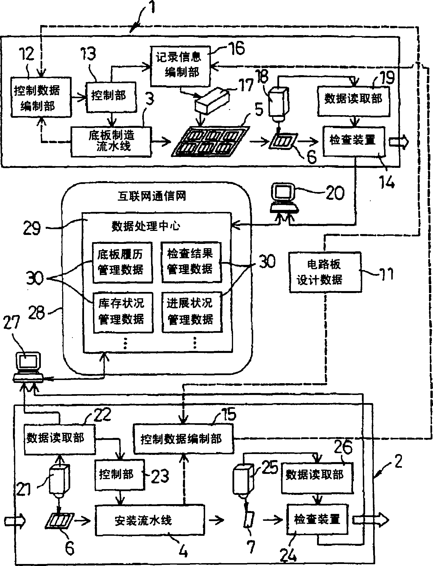
[0022] Below, refer to Figure 1 to Figure 3 A production method and system implementation of a circuit board of the present invention are described.

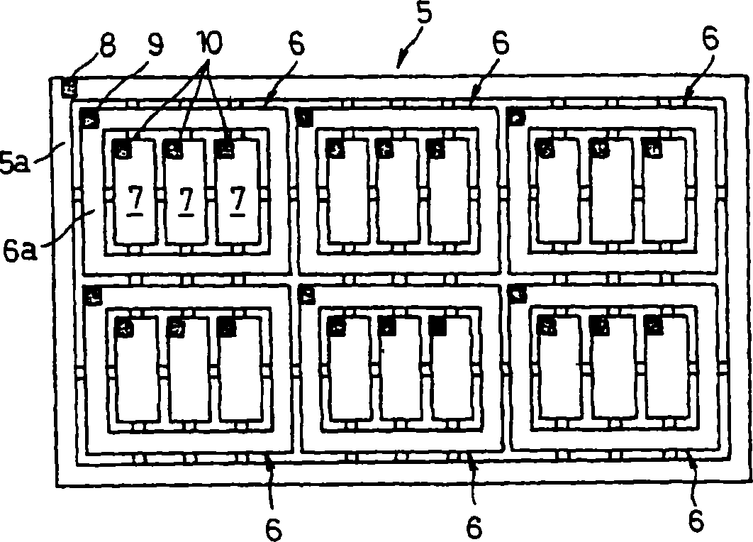
[0023] like figure 1 As shown, in the present embodiment, in the backplane manufacturing line 3 of the backplane manufacturing plant 1, a large multi-piece backplane (hereinafter referred to as a backplane block) 5 in which a plurality of backplanes are arranged is manufactured, and is divided into a plurality of pieces arranged to become each circuit board. The bottom plate (hereinafter referred to as the bottom plate piece) 6 of the bottom plate (hereinafter referred to as the bottom plate piece) is circulated to the installation plant 2 and supplied to the plant, and the installation line 4 of the installation plant 2 installs the required base plate pieces 7 of the bottom plate piece 6. The electronic components are further divided into respective base parts 7 to produce circuit boards.

[0024] like figure 2As shown, t...


PUM


Abstract

There is provided a circuit substrate manufacturing method for manufacturing a circuit substrate in two steps: the first step for manufacturing a substrate at a substrate manufacturer (1) and the second step for mounting electronic parts on the substrate for manufacturing a circuit substrate at a mounting manufacturer (2). At one or more division stages, the substrate board (5) is divided via substrate sheets (6) to substrate pieces (7). By using the substrate board (5), identification information consisting of information associated with the entire substrate board and information indicating relative relationship by divisions at each division stage is recorded on respective information recording units (8, 9, 10) arranged to correspond to the substrates before and after the division at each division stage before the substrates are delivered from the substrate manufacturer (1) to the mounting manufacturer (2). By referencing the identification information, it is possible to easily trace the history, i.e., trace a manufacturing progress of the circuit substrate divided and a manufacturing history when a defect is caused while increasing the productivity of the circuit substrate by using the multi-piece substrate.

Description

technical field [0001] The invention relates to a method and system for producing a circuit board, in particular to a multi-part backplane that is divided in one or more division stages by a backplane manufacturer and is properly divided, and then circulated to an installation factory to be installed with electronic components. A circuit board production method and system for producing a circuit board as well as a multi-component base plate and circuit board thereof. Background technique [0002] Conventionally, in the production of circuit boards for various electronic devices, design data of a backplane based on circuit board design data is supplied to a backplane manufacturer. The backplane is produced at the backplane manufacturing plant based on the backplane design data. At this time, for production management and distribution management, the chassis manufacturer independently writes its identification information in batch units and individual chassis units. Next, th...

Claims


Application Information

Patent Timeline
Patent Type & Authority Applications(China)
IPC IPC(8): G05B19/418H01L23/544H05K1/02H05K3/00
CPCH05K2201/09936H01L23/544H05K3/0052H05K1/0266H01L2223/54473H01L2924/0002H01L2924/00G05B19/418H05K1/02H05K3/00
Inventor 小林德实
Owner PANASONIC CORP
Why Eureka
Try Eureka