Packaged semiconductor grain

A packaging structure, semiconductor technology, applied in the direction of semiconductor devices, semiconductor/solid-state device components, electric solid-state devices, etc., can solve the problems of not mentioning testing and reducing cost chip pads, not mentioning new pad design and other problems

Inactive Publication Date: 2007-02-28
ETRON TECH INC
View PDF5 Cites 13 Cited by
  • Summary
  • Abstract
  • Description
  • Claims
  • Application Information

AI Technical Summary

Problems solved by technology

In prior art U.S. Patent Nos. US6,326,801 (Littlebury), US5,012,187 (Yasuda et al.), US6,469,327 (Loughmiller et al.), US6,396,300, and US4,685,998 (Quinn et al.), all disclose Various contact pad designs have been proposed, but the new pad design contained in the present invention has not been mentioned in the above-mentioned arts, especially the design of chip pads for improving testing and reducing costs has not been mentioned.

Method used


Image

  • Packaged semiconductor grain
  • Packaged semiconductor grain
  • Packaged semiconductor grain

Examples


Embodiment Construction

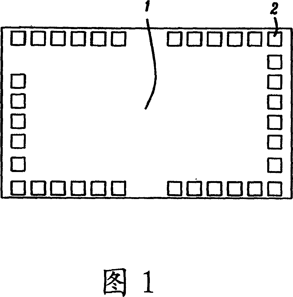
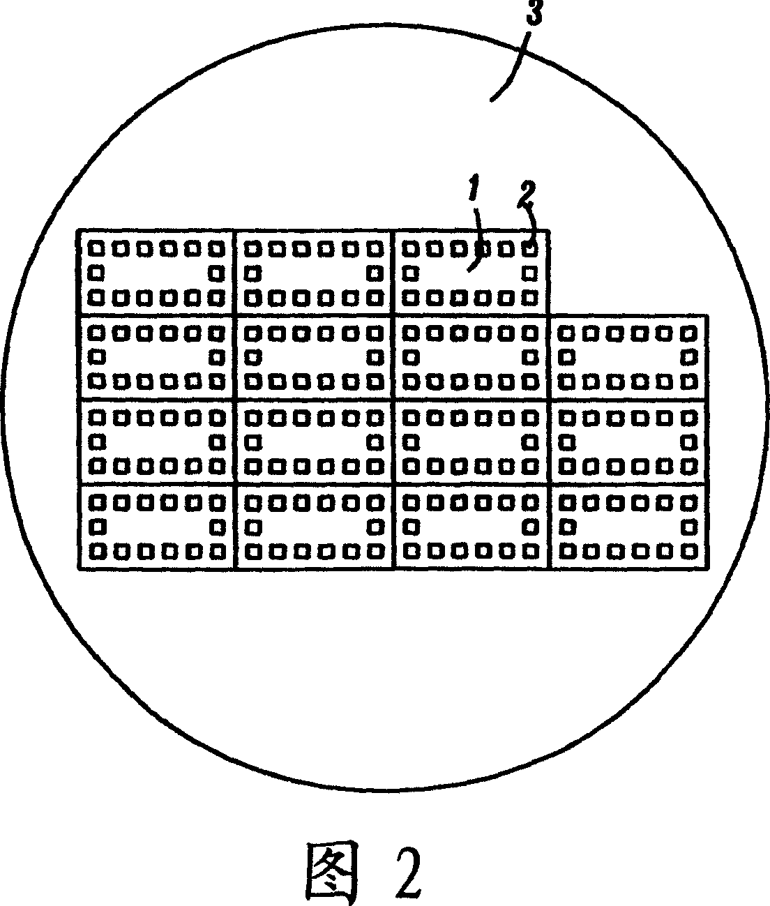
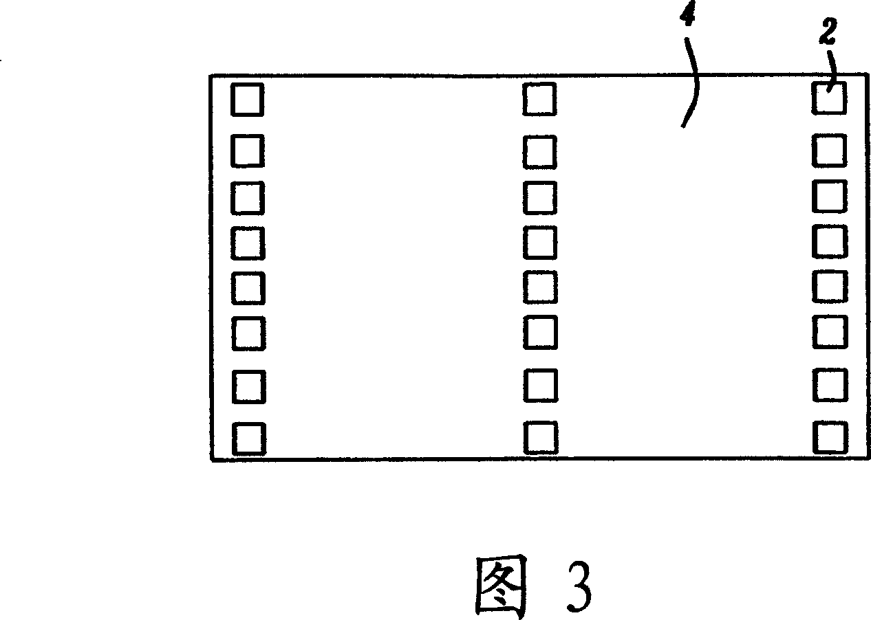
[0014] A semiconductor chip is obtained by forming a specific pattern or design of a circuit or device on a specific area of ​​a semiconductor substrate or wafer, and replicating these specific patterns or device designs on the semiconductor wafer to produce more of the same Structure. Each semiconductor chip is composed of active components formed on a semiconductor wafer and an overlying conductive circuit connecting the active components to generate an array of components and circuits required by the designer. The covering conductive circuit includes a plurality of metal interconnect structures, and these metal interconnect structures are finally terminated near the topmost surface of the semiconductor chip, so as to connect the component circuit in the semiconductor substrate with the external package (package) Solder or connect. The characteristic of the semiconductor chip is that its surface has pad structures, and these pad structures are used as the interface between ...


PUM


Abstract

A semiconductor die featuring vertical rows of bonding pad structures is disclosed. The rows of bonding pad structures are located vertically in the Y direction, or traversing the width of the semiconductor die. A vertical row of bonding pad structures is located on each side of the semiconductor die while a third vertical row of bonding pad structures is located in the center of the semiconductor die. A first set of wire bonds connect each bonding pad structure located on the sides of the semiconductor die to a conductive lead structure located on a ceramic package. A second set of wire bonds connect each bonding pad structure located in the center of the semiconductor die to a lead on chip (LOC) structure located on the semiconductor die. The configuration of only vertical rows of bonding pad structures allows optimized parallel testing of the completed semiconductor chip to be accomplished when compared to testing performed on a semiconductor chip featuring both vertical and horizontal rows of bonding pad structures located on all sides of the semiconductor chip.

Description

technical field [0001] The invention relates to a method for manufacturing and testing a semiconductor chip, in particular to a pad design for a semiconductor chip or crystal grain, thereby realizing the best test of the semiconductor chip or crystal grain. Background technique [0002] The semiconductor industry continues to increase the performance of semiconductor chips while reducing the cost of manufacturing or processing those chips. Manufacturing cost reductions have been achieved by eliminating or integrating specific process steps or stages, such as directly depositing a doped semiconductor layer instead of the more time-consuming process of depositing a pure semiconductor material layer followed by doping. complex two-stage procedure. In addition, the development of advanced semiconductor equipment such as rapid thermal processing (rapid thermal processing (RTP)) also reduces the time required for a specific process. On the other hand, however, testing of the ent...

Claims


Application Information

Patent Timeline
Patent Type & Authority Applications(China)
IPC IPC(8): H01L23/488H01L23/485
CPCH01L2924/01082H01L2224/4826H01L2224/48644H01L23/4951H01L2924/01029H01L2224/48453H01L2224/06136H01L2224/48091H01L2924/01013H01L2224/48464H01L2924/01024H01L24/48H01L2224/05644H01L24/45H01L2224/48599H01L24/06H01L2224/4845H01L2924/10157H01L2924/01079H01L2224/4807H01L24/05H01L2224/48647H01L2224/48227H01L2224/04042H01L2224/05647H01L2924/01033H01L2224/05157H01L2224/06135H01L2224/45144H01L2924/12044H01L2224/05554H01L2924/00014H01L2924/00
Inventor 夏浚
Owner ETRON TECH INC
Why Eureka
Try Eureka