Gap-type printed circuit board radiating layout
A printed circuit board, gap-type technology, applied in the field of design and layout of printed circuit boards, can solve problems such as reduced efficiency, increased cost and energy consumption, and does not adapt to the development trend of miniaturization of electronic products, so as to increase the design margin , the effect of simple structure
- Summary
- Abstract
- Description
- Claims
- Application Information
AI Technical Summary
Problems solved by technology
Method used
Image
Examples
Embodiment
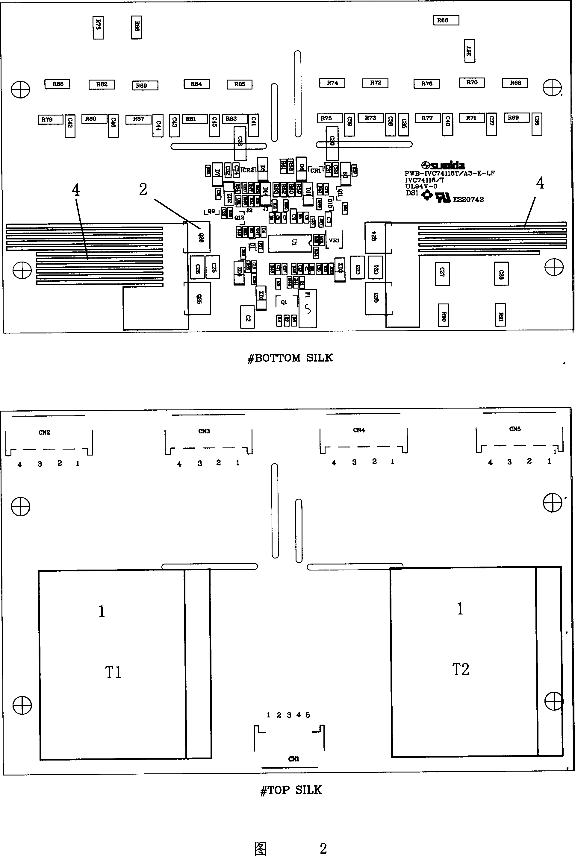
[0016] Referring to Fig. 2, it is the bottom layer and the top layer design of the printed circuit board of the cold-cathode tube drive module named IV74116-Z-LF product name 1554Z002 for the model of the embodiment of the present invention, and the making of this circuit board can be realized by existing circuit board manufacturing technology . The heat dissipation layout 4 designed on both sides of the bottom layer is a straight line grid-shaped copper foil, and the corresponding copper foil structure inside the circuit board is also a straight line grid structure. The heating element 2 includes Q23, Q24, Q25 and Q26 respectively connected to the heat dissipation layout 4 on both sides, all of which are MOS (field effect transistors), and two transformers 1 are respectively arranged on both sides of the top layer, the codes are respectively T1 and T2, The heat dissipation layout of the MOS is directly below the transformer.
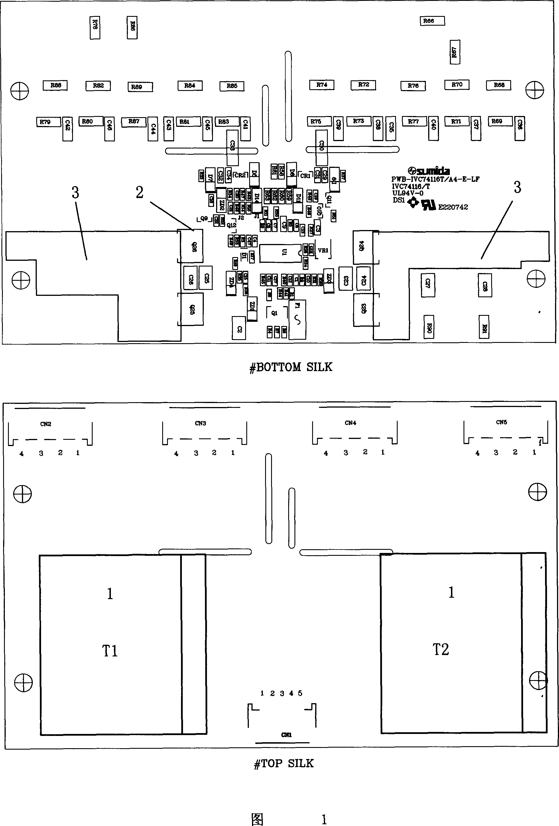
[0017] Referring to Fig. 1, it is a cold-cathode...
PUM
 Abstract
Description
Claims
Application Information


