Induced quantity compensating method of touch controlling board inductor

A compensation method and sensor technology, applied in the input/output process of instruments, data processing, electrical digital data processing, etc., can solve the problems of calculation object position offset, action misjudgment, etc., and achieve the effect of avoiding offset

Inactive Publication Date: 2007-04-18
ELAN MICROELECTRONICS CORPORATION
View PDF0 Cites 5 Cited by
  • Summary
  • Abstract
  • Description
  • Claims
  • Application Information

AI Technical Summary

Problems solved by technology

It can be known from formula 2 that when the object is operated on the sensor 100, the inductances generated at different positions are different due to the different basic capacitances of the traces. As shown in F

Method used


Image

  • Induced quantity compensating method of touch controlling board inductor
  • Induced quantity compensating method of touch controlling board inductor
  • Induced quantity compensating method of touch controlling board inductor

Examples


Embodiment Construction

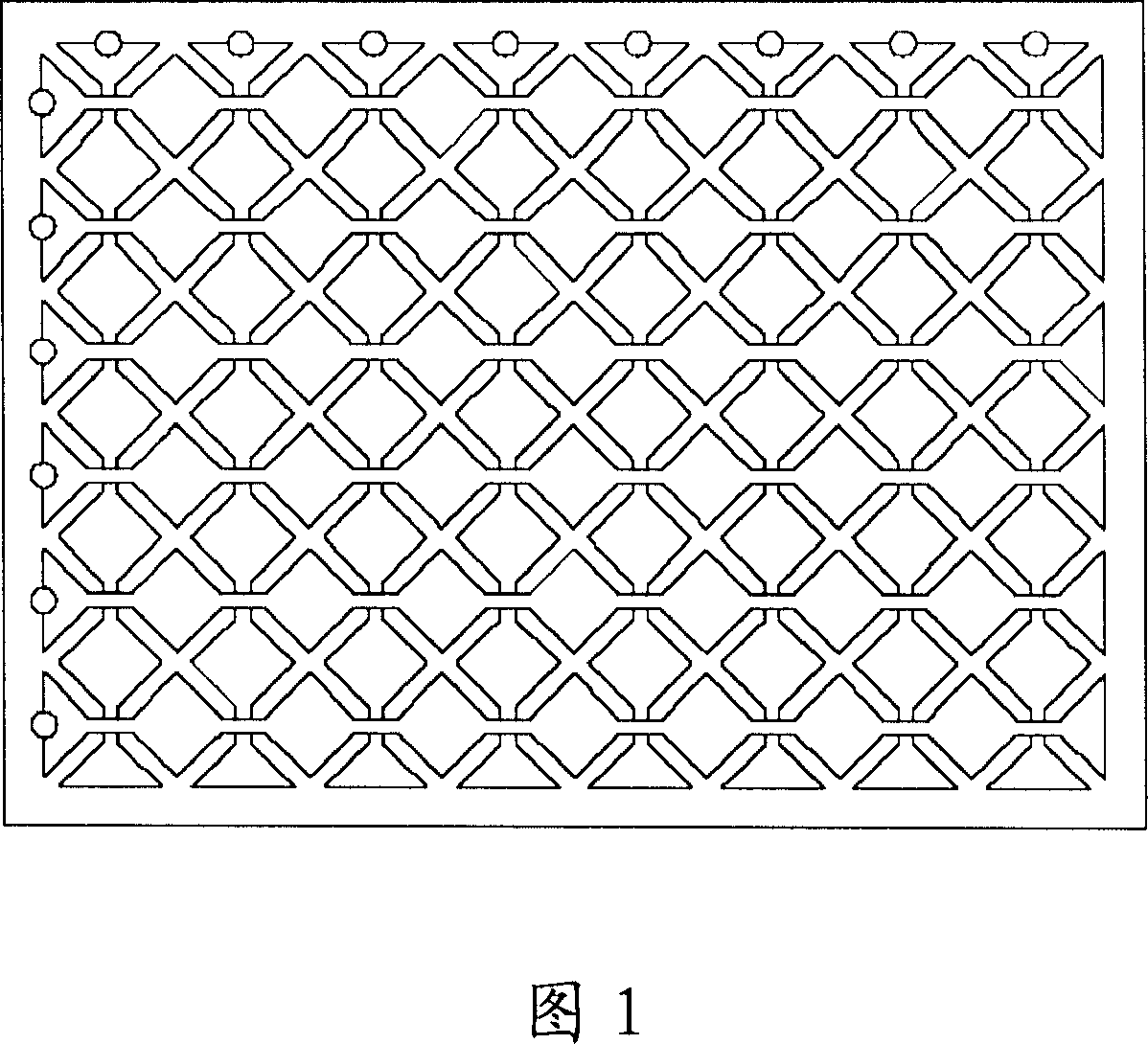
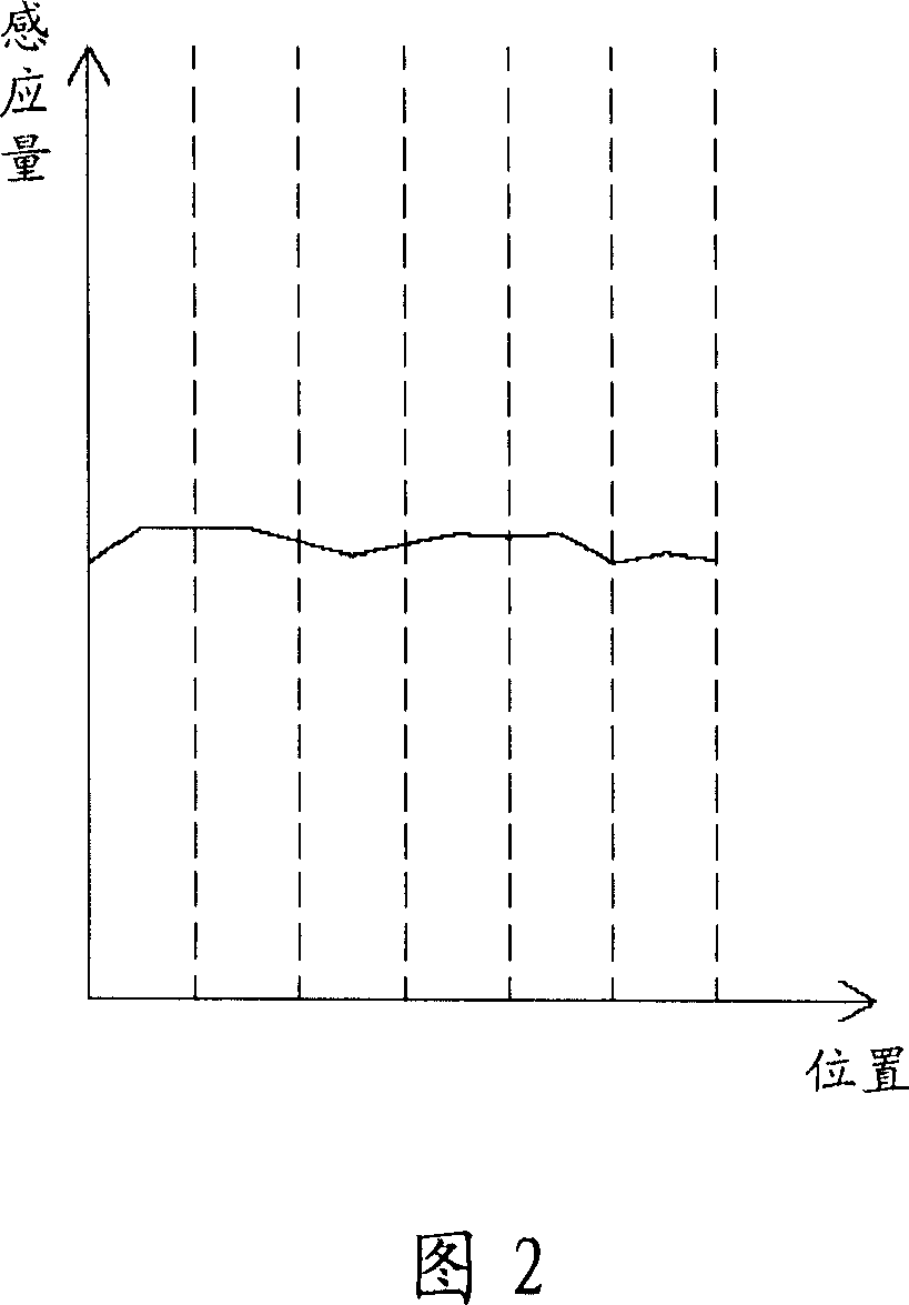
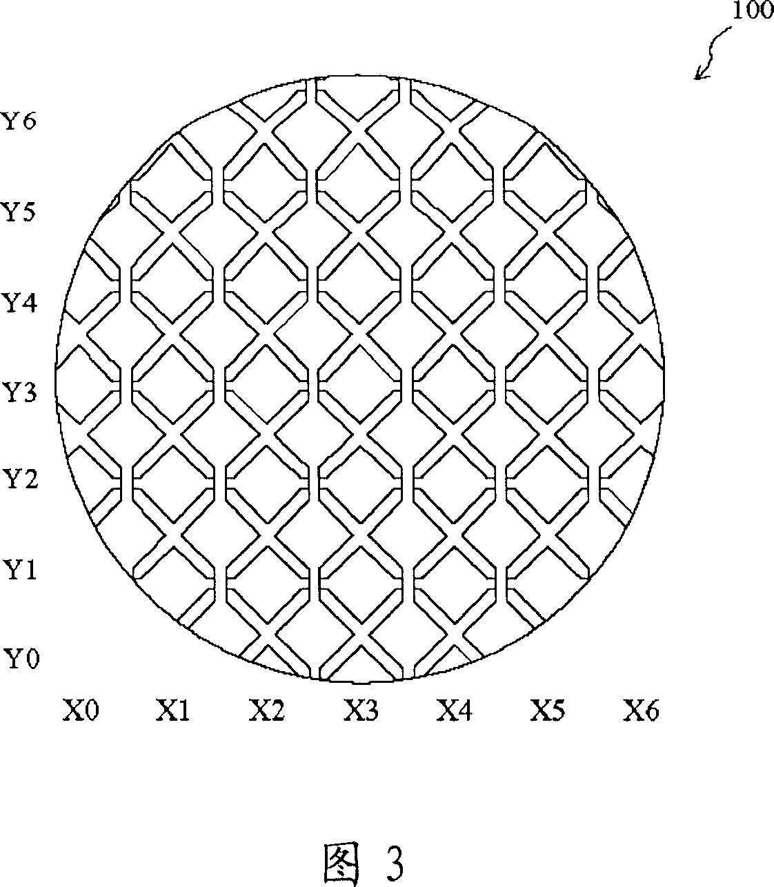
[0056] FIG. 5 is a flowchart 200 of an embodiment of the present invention. Step 210 calculates the basic capacitance C of the first and second traces according to formula 1. 1 and C 2 , step 220 calculates the basic capacitance C of the first and second traces 1 and C 2 The capacitance difference ΔC, the one with the larger basic capacitance minus the one with the smaller basic capacitance, for example, ΔC=C 1 -C 2 , step 230 is equal to a compensation area A according to the capacitance difference ΔC 0 Generated basic capacitance, calculate a compensation area A 0 size, A 0 =ΔC*(d 0 / ε), d 0 for A 0 The distance from the ground plane, ε is the permittivity, and in step 240 the compensation area A 0 Connecting to a trace with a smaller basic capacitance, such as connecting to a second trace, so that the first and second traces have the same basic capacitance, wherein the first and second traces can be located on the same sensing layer or different sensing layers, whe...


PUM


Abstract

The invention relates to touch pad inductor inducing rate compensating method. It includes the following steps: computing the relationship between the compensating area or line trace area and the ground plane distance; adjusting the line trace area or ground plane position to make the different line traces have equal basic capacity.

Description

technical field [0001] The invention relates to a touch panel, in particular to a method for compensating the inductance of a sensor of the touch panel. Background technique [0002] Due to its small size, low cost, low power consumption and long service life, touchpads are widely used in various electronic products, such as notebook computers, mice, MP3 players, and even mobile phones, as input devices. Users only need to slide or touch objects (such as conductive objects such as fingers or stylus pens) on the panel to make the cursor move relative or with absolute coordinates to complete text writing, scrolling windows and virtual buttons. and other inputs. Most of the known touch panel sensors have a symmetrical structure, such as the square structure shown in FIG. It is symmetrical, and the sensing amount caused by the object on the touch panel sensor is also symmetrical and linearly equal, as shown in FIG. 2 . However, as the application is different, the shape and s...

Claims


Application Information

Patent Timeline
IPC IPC(8): G06F3/044
Inventor 李文凯汤冠群
Owner ELAN MICROELECTRONICS CORPORATION
Why Eureka
Try Eureka