Liquid crystal display, and driving method
A technology of liquid crystal display and driving method, which is applied in the field of color sequential liquid crystal display and its driving, and can solve problems such as drift and uneven brightness of liquid crystal display panels
- Summary
- Abstract
- Description
- Claims
- Application Information
AI Technical Summary
Problems solved by technology
Method used
Image
Examples
no. 1 example
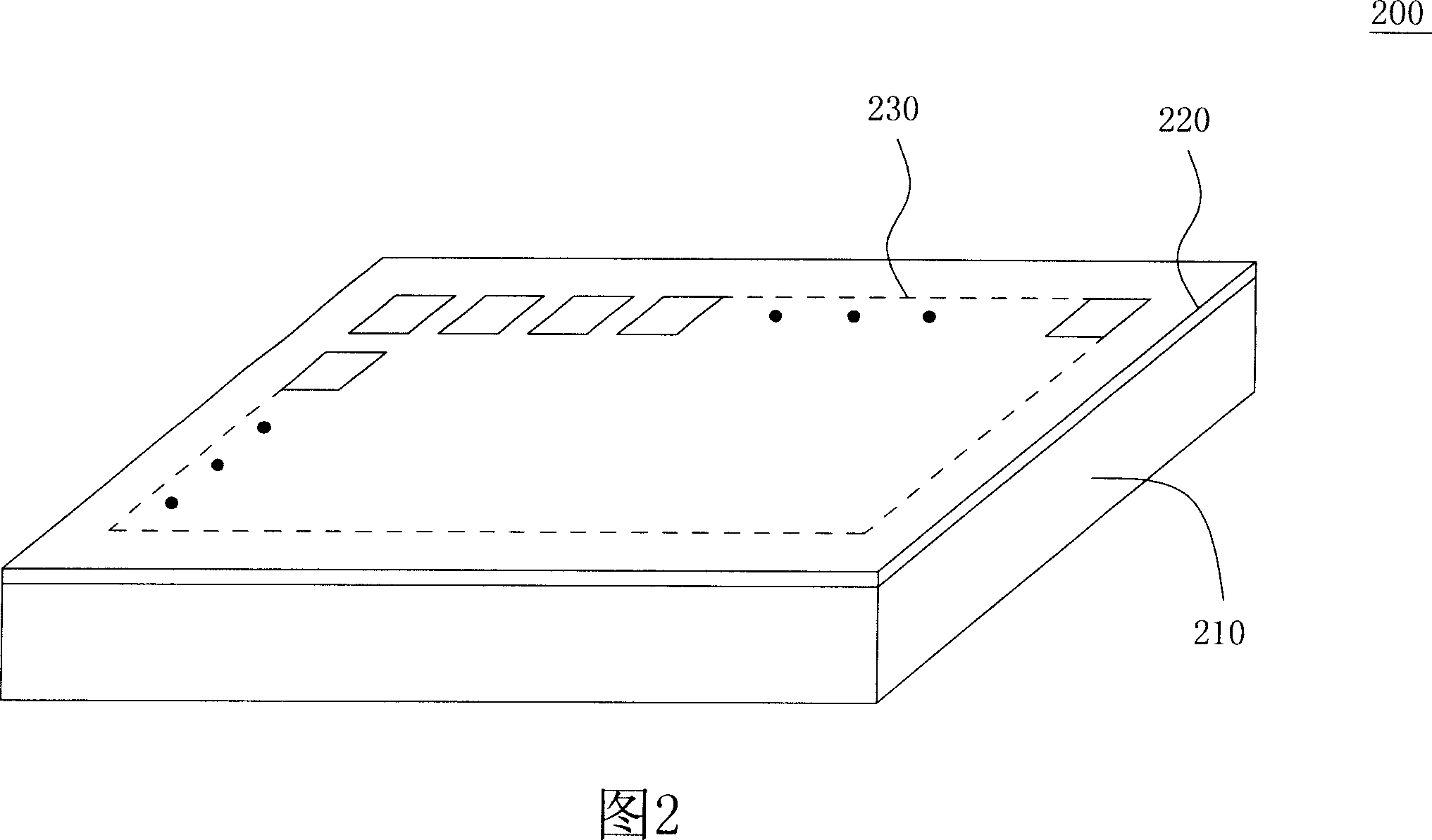
[0049] Referring to FIG. 2 , it is a schematic diagram of a liquid crystal display according to a first embodiment of the present invention. Referring to FIG. 3 at the same time, it is a schematic diagram of a pixel array according to a first embodiment of the present invention. The liquid crystal display 200 includes a backlight module 210 and a liquid crystal display panel 220 having a pixel array 230 . The pixel array 230 includes a plurality of pixel columns L1 ˜ Ln, the pixels of which are respectively coupled to the scan driving circuit 240 through the scan lines 242 and coupled to the data driving circuit 250 through the data lines 252 . The scanning driving circuit 240 is used for providing the scanning voltage to the pixel, and the data driving circuit 250 is used for providing the pixel voltage to the corresponding pixel so as to change the light transmittance of the pixel.
[0050]Referring to FIG. 4 , it is a flowchart of a driving method of a liquid crystal displ...
no. 2 example
[0058] Referring to FIG. 7A , it is a schematic diagram of a liquid crystal display according to a second embodiment of the present invention. Different from the first embodiment, in the liquid crystal display panel 700 , the display area of the pixel array 710 is divided into a plurality of sub-display areas A1 -An. Each sub-display area includes a plurality of columns of pixels, and these pixels are respectively coupled to the scan driving circuit 720 and the data driving circuit 730 . In addition, one end of the storage capacitors of multiple columns of pixels in the first sub-display area A1 is coupled to the first common electrode line CL1, (the label of the line belongs to the label of the line, and the code of the signal belongs to the code of the signal) The second sub-display area A2 One end of the storage capacitors of multiple columns of pixels is coupled to the second common electrode line CL2, and so on, one end of storage capacitors of multiple columns of pixel...
PUM
 Abstract
Description
Claims
Application Information


