Active matrix display devices

An active matrix, display device technology, applied in static indicators, instruments, etc., can solve the problem of not prolonging the life of the display

Inactive Publication Date: 2007-05-16
KONINKLIJKE PHILIPS ELECTRONICS NV
View PDF2 Cites 7 Cited by
  • Summary
  • Abstract
  • Description
  • Claims
  • Application Information

AI Technical Summary

Problems solved by technology

[0015] Although known pixel circuits, and especially those described generally above (and also in detail below), can provide correction for differential aging of LED display elements of different pixels, they do not extend the lifetime of the display

Method used


Image

  • Active matrix display devices
  • Active matrix display devices
  • Active matrix display devices

Examples


Embodiment Construction

[0052] It should be understood that the drawings described above are schematic and not shown to scale. For clarity and convenience of the drawings, relative sizes and proportions of parts of the above-mentioned drawings have been exaggerated or reduced.

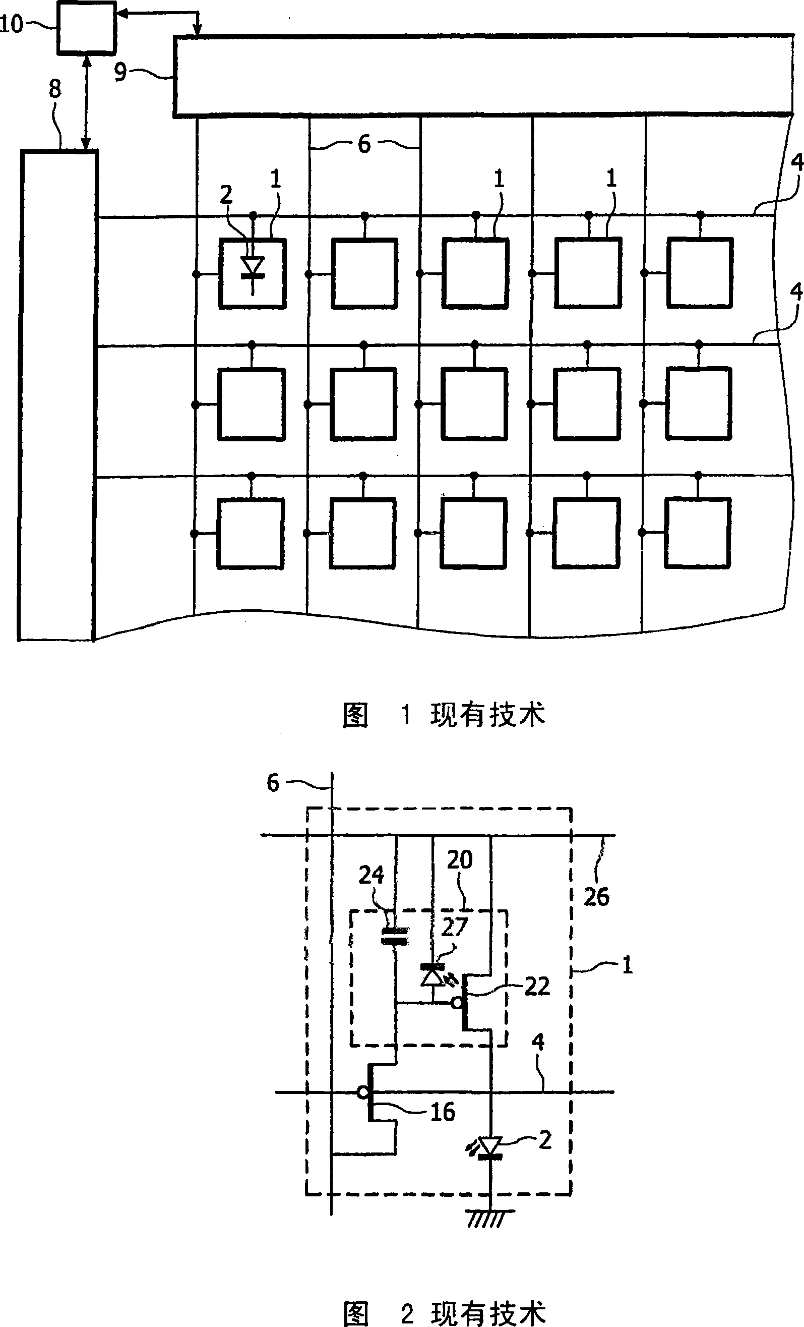
[0053] A pixel circuit that has been proposed by the applicant (but not published before the filing date of this application) will be described first. In the pixel circuit described above, a constant gate voltage is used during the specified frame period and the time period during which the display element emits light (at constant brightness) taking into account aging effects caused by both the LED material and the drive transistor, and the desired brightness output. drive the drive transistor.

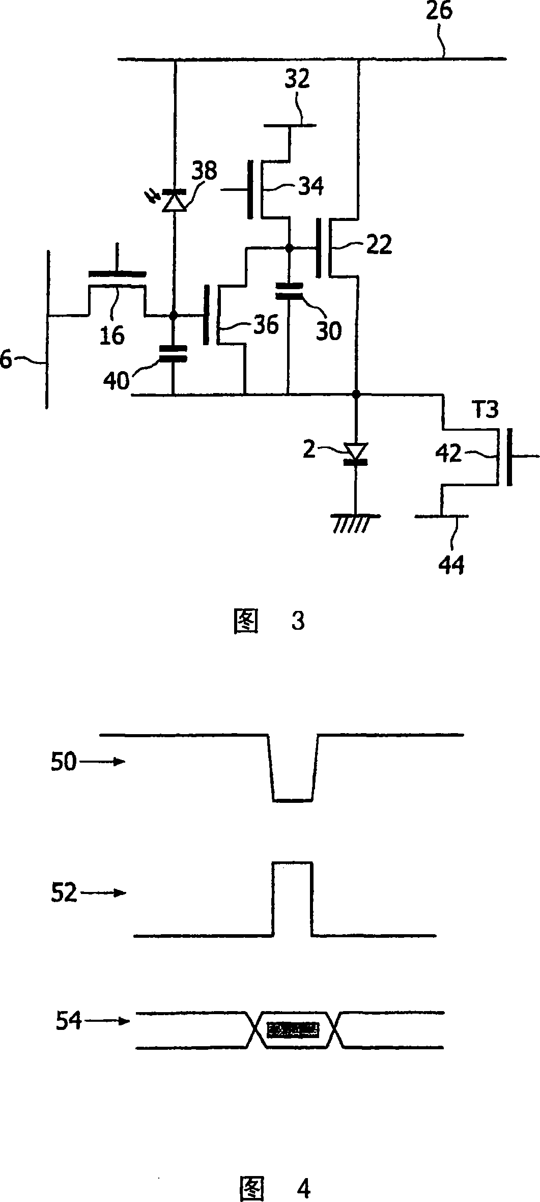
[0054] Figure 3 shows an example of the proposed pixel structure. Pixel circuits are used in displays such as that shown in FIG. 1 . The circuit of Figure 3 is suitable for implementation using amorphous silicon n-type transistors...


PUM


Abstract

An active matrix display device has an array of display pixels, each pixel comprising a current-driven light emitting display element (2), a drive transistor (22) for driving a current through the display element and pixel circuitry including an optical feedback element (38), for controlling the drive transistor to drive a substantially constant current through the display element for a duration which depends on the desired display pixel output level and an optical feedback signal of the optical feedback element. An output configuration is applied to the display which includes values for the pixel power supply voltages, the field period and an allowed range of pixel drive levels. The output configuration is varied in response to ageing of the display element. In this device, an output configuration is varied as the device ages, so that the optical feedback system can continue to provide compensation for differential ageing of the display elements for a longer period of use of the display.

Description

technical field [0001] The present invention relates to an active matrix display device, in particular but not exclusively to an active matrix electroluminescent display device having a thin film switching transistor associated with each pixel. Background technique [0002] Matrix display devices using electroluminescent light-emitting display elements are known. Display elements may include organic thin film electroluminescent elements, such as those employing polymeric materials, or other light emitting diodes (LEDs) employing conventional III-V semiconductor compounds. In the current development of organic electroluminescent materials, polymeric materials in particular have shown their capabilities especially for use in video display devices. Such materials typically comprise one or more layers of semiconducting conjugated polymers sandwiched between a pair of electrodes, one of which is transparent and the other is formed with a material suitable for injecting holes or ...

Claims


Application Information

Patent Timeline
Patent Type & Authority Applications(China)
IPC IPC(8): G09G3/32G09G3/20
CPCG09G3/2014G09G2330/021G09G2300/0417G09G2320/0285G09G2320/045G09G2320/0295G09G2300/0852G09G2300/0861G09G2320/043G09G2310/0251G09G3/3233G09G2320/0233G09G2300/0819G09G2360/148
Inventor D·A·菲什
Owner KONINKLIJKE PHILIPS ELECTRONICS NV
Why Eureka
Try Eureka