

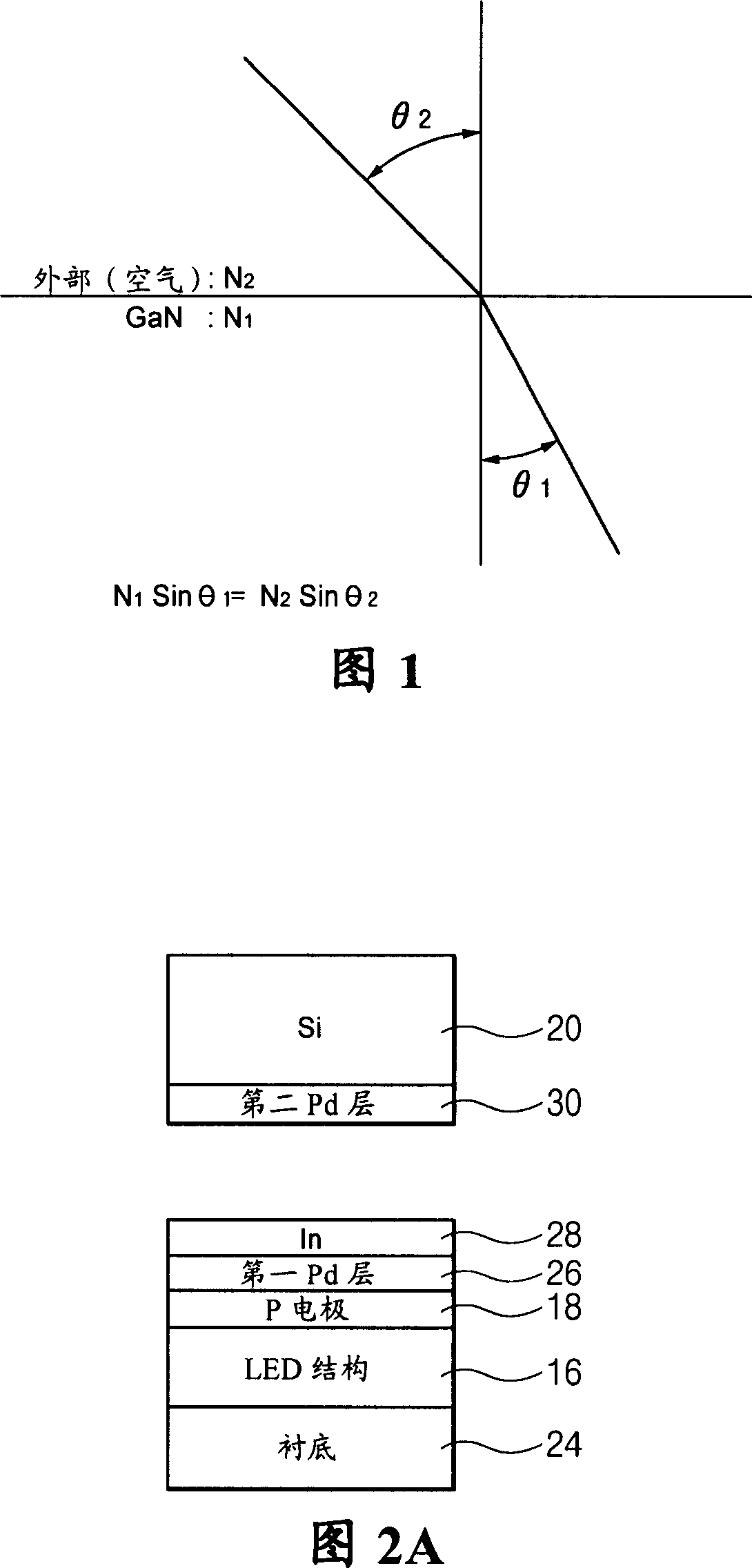
Vertically structured gan type led device
A technology of light-emitting diodes and gallium nitride, which is applied to electrical components, circuits, semiconductor devices, etc., to achieve the effect of maximizing external quantum efficiency
- Summary
- Abstract
- Description
- Claims
- Application Information
AI Technical Summary
Problems solved by technology
Method used
Image

Examples
change example 1
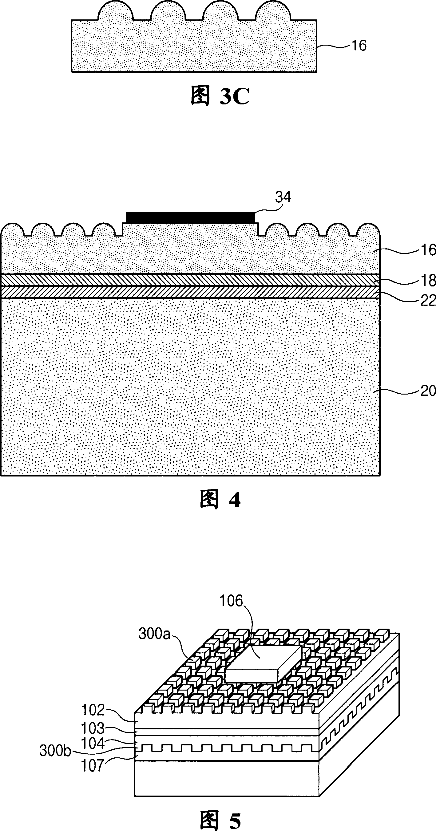
[0056] Next, a first unevenness pattern according to a first modified example of the present invention will be described in detail with reference to FIG. 7 .
[0057] 7 is a plan view illustrating an arrangement of a first uneven pattern according to a first modified example of the present invention.
[0058] Referring to FIG. 7, the first uneven pattern 300a is a polygonal structure in which one or more polygons are periodically arranged on the surface of the n-type GaN layer 102 in contact with the n-electrode 106 and are spaced apart from each other by a predetermined distance.
[0059] In particular, adjacent polygons are preferably separated by a distance equal to or greater than the wavelength of light emitted from the active layer in order to improve the refraction characteristics of light emitted from the LED. For example, when blue light is emitted from the active layer 103, since the wavelength of the blue light is in the range of about 400 nm to about 450 nm, the li...
change example 2
[0063] Next, a first unevenness pattern according to a second modified example of the present invention will be described in detail with reference to FIG. 8 .
[0064] FIG. 8 is a plan view illustrating an arrangement of a first uneven pattern according to a second modified example of the present invention.
[0065] Referring to FIG. 8, the first uneven pattern 300a has a diffraction structure in which one or more lines are periodically arranged in the same direction and are spaced apart from each other by a predetermined distance. In particular, adjacent lines are preferably separated by a distance equal to or greater than the wavelength of light emitted from the active layer in order to improve the refraction characteristics of light emitted from the LED.
[0066] In addition, a line including the first uneven pattern 300a having a diffractive structure may be a straight line, a curved line, or a single closed curve. That is, as shown in FIG. 8, the first uneven pattern 300...
change example 3
[0068] Next, a first unevenness pattern according to a third modified example of the present invention will be described in detail with reference to FIG. 9 .
[0069] FIG. 9 is a plan view illustrating an arrangement of a first uneven pattern according to a third modified example of the present invention.
[0070] Referring to FIG. 9, the first uneven pattern 300a has a mesh structure in which two or more lines intersect at one or more points. Similar to the second modified example of the present invention, the line including the first uneven pattern 300a having a mesh structure may be a straight line, a curved line, or a single closed curved line.
PUM
 Abstract
Description
Claims
Application Information