Back light module and liquid crystal display device
A technology of backlight module and light source, applied in optics, nonlinear optics, static indicator, etc., can solve the problem of inconvenient assembly of backlight module, and achieve the effect of simplifying assembly steps, convenient assembly, and simple assembly action.
- Summary
- Abstract
- Description
- Claims
- Application Information
AI Technical Summary
Problems solved by technology
Method used
Image

Examples
Embodiment Construction
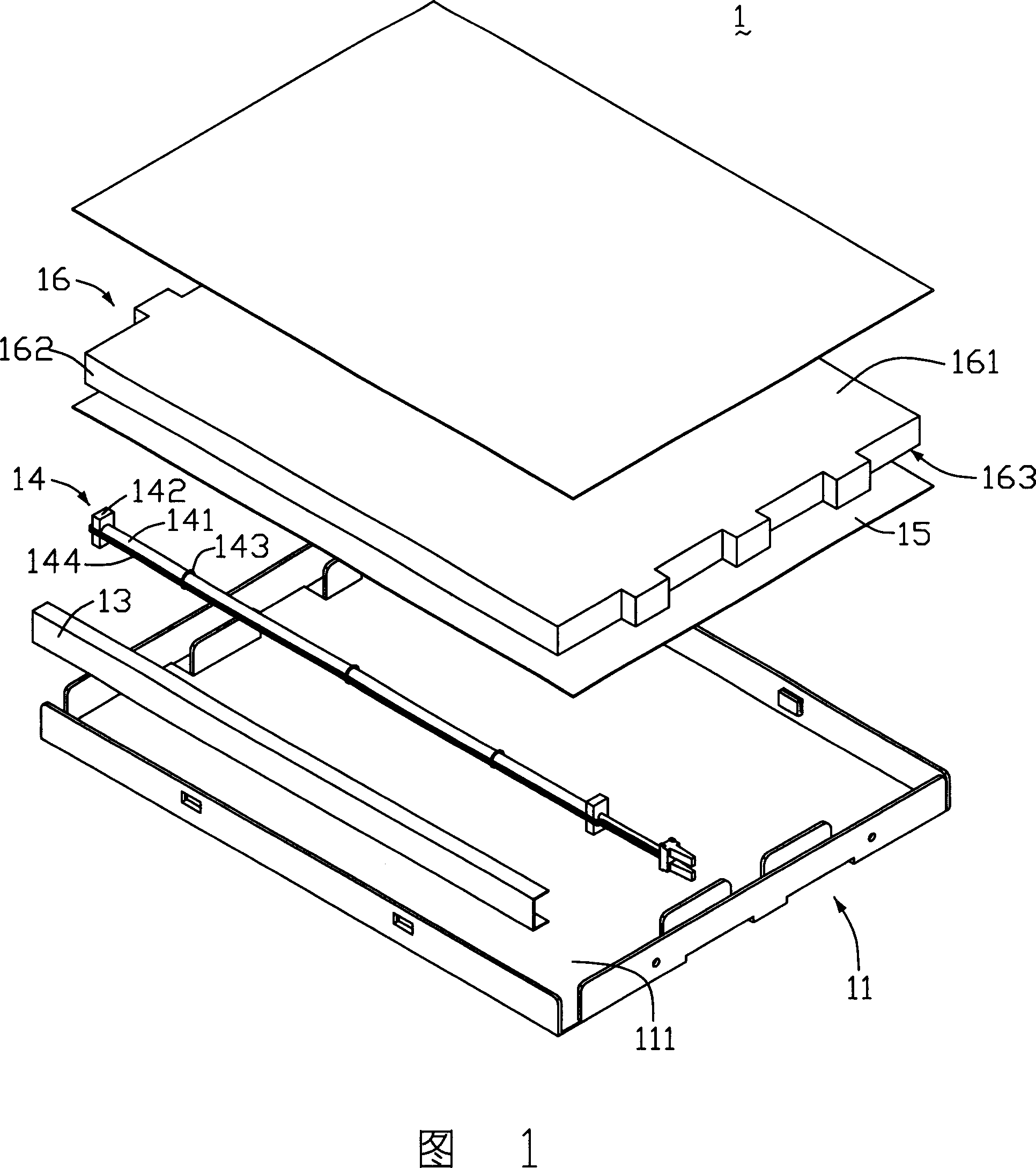
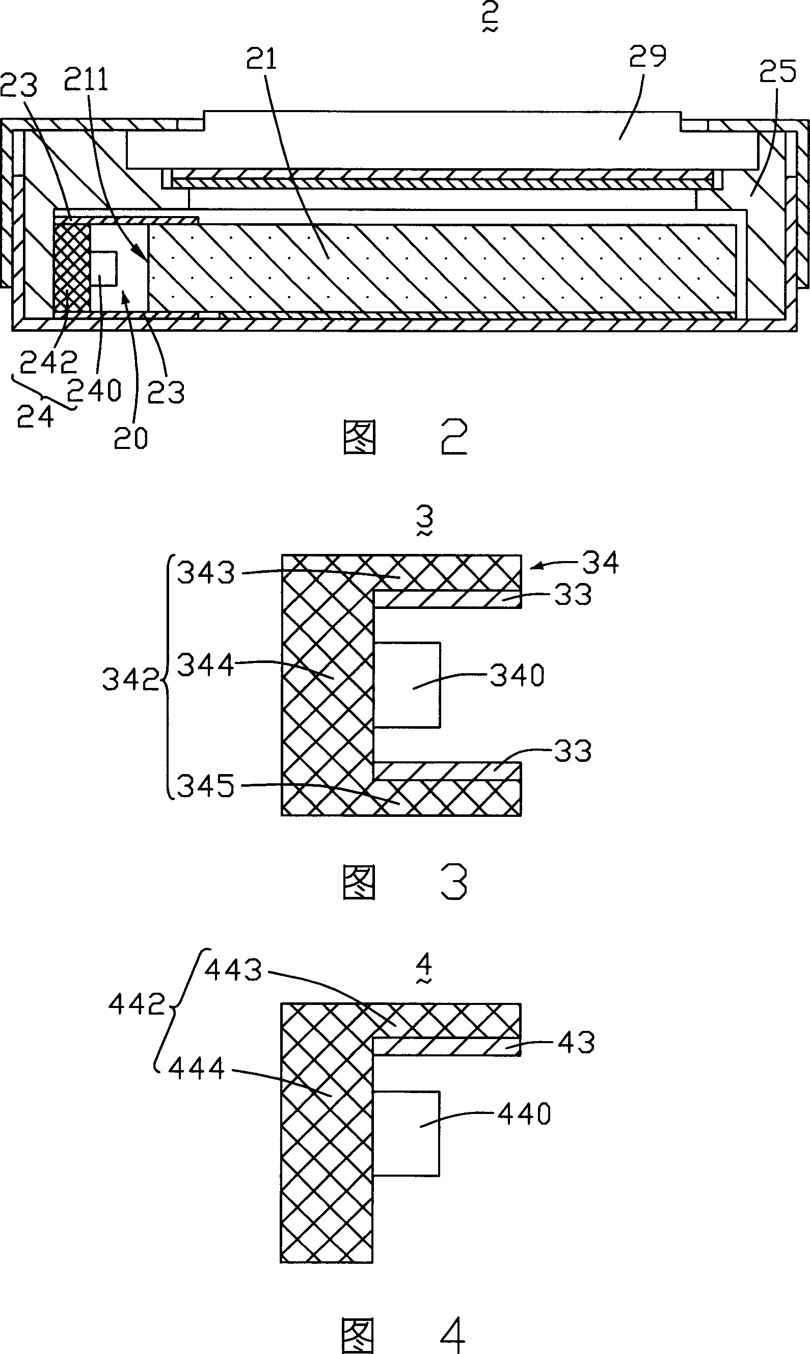
[0018] Please refer to FIG. 2 , which is a cross-sectional view of the first embodiment of the liquid crystal display device of the present invention. The liquid crystal display device 2 includes a backlight module 20 and a liquid crystal panel 29 arranged opposite to the backlight module 20. The backlight module 20 includes a The light guide plate 21 on the light incident surface 211 , a light source 24 disposed adjacent to the light incident surface 211 , and a frame 25 accommodating the light guide plate 21 and the light source 24 .
[0019] The light source 24 includes a strip support 242 , a plurality of LEDs 240 disposed on the strip support 242 , and two reflective elements 23 adjacent to the LEDs 240 . The plurality of LEDs 240 are arranged in a row. The strip-shaped support 242 is a cylinder on which a circuit is arranged, and the external power supply lights up the light-emitting diode 240 through wires (not shown) and the circuit on the strip-shaped support 242 . T...
PUM
 Abstract
Description
Claims
Application Information
PatSnap Eureka turns technology decisions into work you can execute. Powered by our Innovation Knowledge Graph, it runs expert workflows across engineering, life sciences, materials and intellectual property. Get your review-ready output in minutes.


