Method of testing wires and apparatus for doing the same

A wiring and bad technology, applied in the direction of measuring devices, instruments, measuring electricity, etc., can solve the problem of grid wiring 1002 disconnection and so on

Inactive Publication Date: 2007-07-11
NEC LCD TECH CORP
View PDF1 Cites 8 Cited by
  • Summary
  • Abstract
  • Description
  • Claims
  • Application Information

AI Technical Summary

Problems solved by technology

[0004] However, in the conventional pixel storage capacitance detection method, since the storage capacitance of the pixel portion 1007 on the TFT substrate 1000 is detected to detect point defects and line defects, there is a so-called inability to detect defects where the pixel portion 1007 is not formed. The problem of disconnection of the gate wiring 1002 in the state

Method used


Image

  • Method of testing wires and apparatus for doing the same
  • Method of testing wires and apparatus for doing the same
  • Method of testing wires and apparatus for doing the same

Examples


Embodiment Construction

[0052] Hereinafter, embodiments according to the present invention will be described with reference to the drawings.

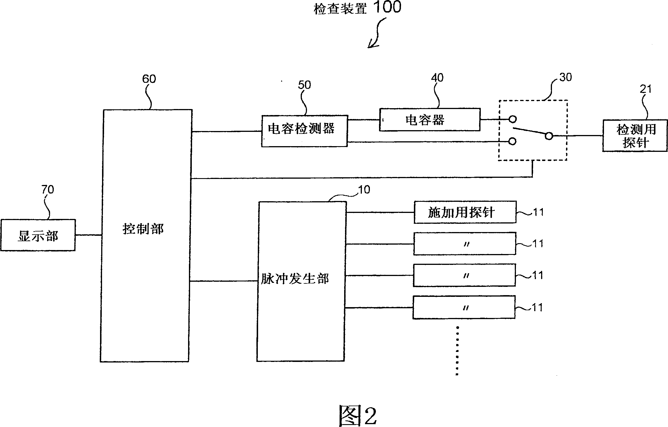
[0053] In this embodiment mode, an inspection device and an inspection method for detecting a disconnection and a short circuit of a gate wiring formed on a TFT substrate will be described.

[0054] First, the structure of a TFT substrate having a gate wiring to be inspected will be described.

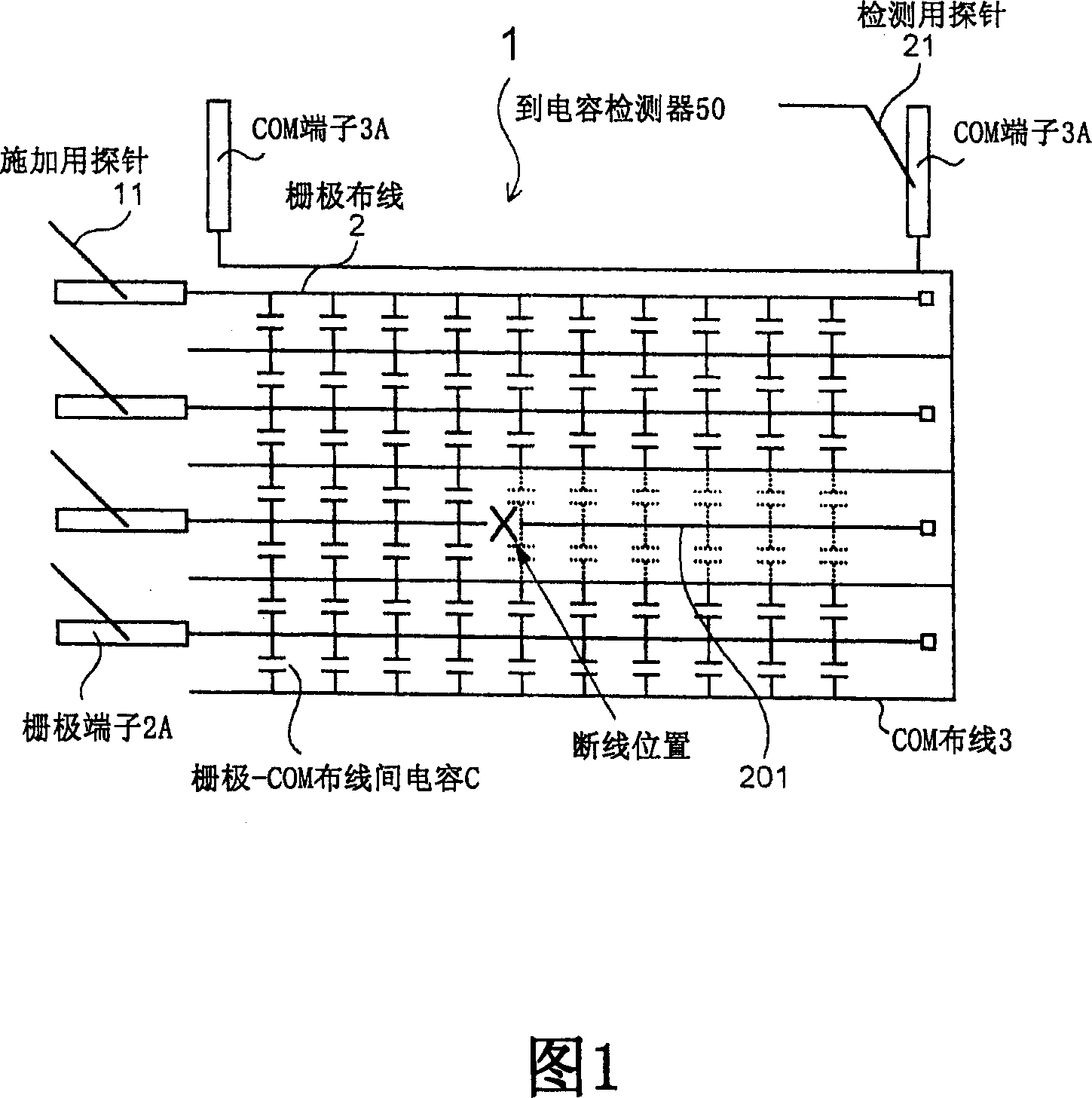
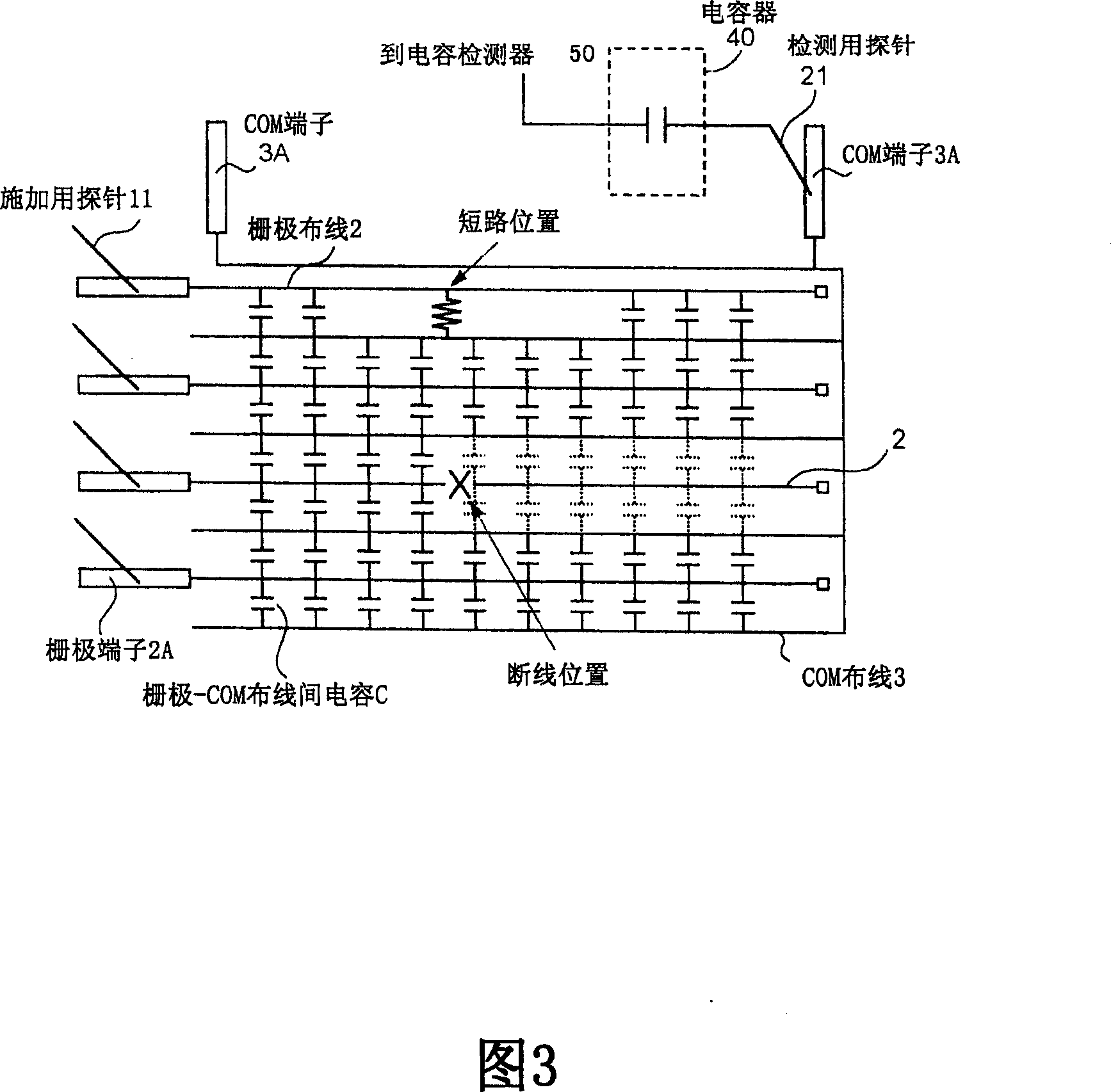
[0055] FIG. 1 is a typical plan view showing the structure of a TFT substrate on which gate wiring and COM wiring are formed.

[0056]As shown in FIG. 1 , a plurality of COM wirings (second wirings) 3 and a plurality of gate wirings (first wirings) 2 to be inspected are formed on a TFT substrate 1 .

[0057] The respective gate wirings 2 extend linearly and are arranged in parallel with each other at equal intervals.

[0058] In addition, the COM lines 3 also extend linearly and are arranged in parallel with each other at equal intervals.

[0059] Furthermore, while...


PUM


Abstract

The invention provides an inspection device for detecting a break and short circuit in gate wires on a TFT substrate before forming a pixel part. The inspection device is used for inspecting a defect in the gate wires 2 on the TFT substrate 1 comprising a plurality of gate wires 2 which are inspecting objects, and a plurality of COM wires 3 capable of forming inter-wire capacitance between themselves and the gate wires 2, respectively. The inspection device includes a pulse generation part for impressing the gate wires 1 with a voltage, a capacitance detector 5 for detecting the inter-wire capacitance between the gate wires 2 and the COM wires 3, and capacitance connected between the COM wires 3 and the capacitance detector 5.

Description

technical field [0001] The invention relates to a wiring fault inspection method and a wiring fault inspection device. Background technique [0002] As shown in FIG. 7, in order to inspect the point defect and the line defect of the TFT substrate 1000, by connecting the measuring probes 1003, 1004 with the terminal portions of the drain wiring 1001 and the gate wiring 1002 formed on the TFT substrate (drain terminal 1001A, gate terminal 1002A) to connect the TFT substrate 1000 to an unshown tester (the tester includes a capacitance detector and a control device and constitutes a tester). In this state, a predetermined voltage is applied from the tester to the TFT substrate 1000 to write and read charges to and from the pixel capacitance formed on the TFT substrate 1000 . Thereby, a defective position is detected. This detection method is called pixel retention capacitance detection method. [0003] In addition, as shown in FIG. 8 , in the TFT substrate 2000 before the for...

Claims


Application Information

Patent Timeline
Patent Type & Authority Applications(China)
IPC IPC(8): G01R31/02G01R27/26
CPCH01L2924/0002G09G3/006H01L2924/00
Inventor 鹭山惠
Owner NEC LCD TECH CORP
Why Eureka
Try Eureka