

Thin film material and method of manufacturing the same
A thin-film material and thin-film layer technology, applied in the fields of polycrystalline material growth, chemical instruments and methods, cable/conductor manufacturing, etc., can solve problems such as insufficient improvement, and achieve the effects of excellent surface smoothness and excellent in-plane orientation.
- Summary
- Abstract
- Description
- Claims
- Application Information
AI Technical Summary
Problems solved by technology
Method used
Image

Examples
no. 1 approach
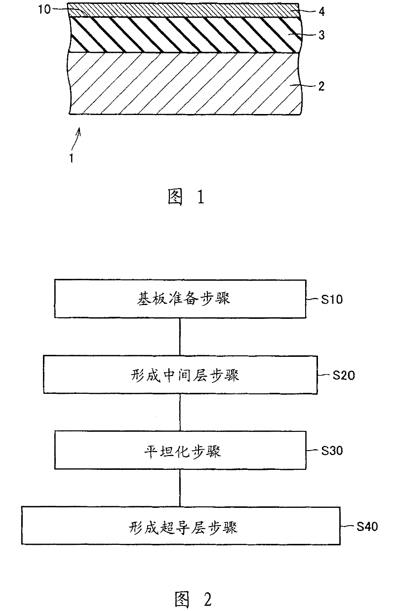
[0038] refer to figure 1 and 2, describe the first embodiment of the superconducting wire rod of the present invention.
[0039] Such as figure 1 As shown, a superconducting wire 1 is composed of a substrate 2 , an intermediate layer 3 and a superconducting layer 4 . The substrate 2 is strip-shaped. The upper surface of the intermediate layer 3 is the polished surface, that is, the polished surface 10 . Therefore, superconducting layer 4 is formed on the upper surface (polished surface 10 ) of intermediate layer 3 having excellent surface smoothness, and thus the surface smoothness and in-plane orientation of superconducting layer 4 are improved. Therefore, superconducting wire 1 exhibiting excellent superconducting properties (critical current value and critical current density) can be obtained.
[0040] Referring then to Figure 2, the fabrication figure 1 The method of superconducting wire 1 is shown. According to manufacture figure 1 In the method of the supercon...
no. 2 approach
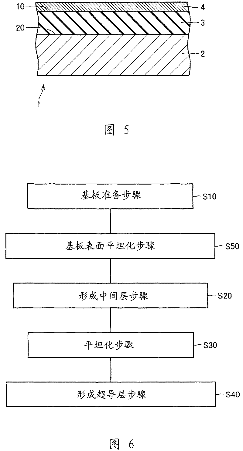
[0053] refer to Figure 5 , to describe the second embodiment of the superconducting wire rod of the present invention.
[0054] Such as Figure 5 As shown, the structure of the superconducting wire 1 is basically the same as figure 1 The superconducting wire 1 shown is similar, except that the upper surface of the substrate 2 is a ground surface 20 that is planarized by grinding. Also in this way, it is possible to provide the same figure 1 A similar effect is shown for the superconducting wire. In addition, since the upper surface of the substrate 2 is also flattened, the in-plane orientation of the superconducting layer 4 formed at the highest level can be further improved. Therefore, the critical current value and critical current density of the superconducting layer 4 can be further increased.
[0055] Referring to Figure 6, the fabrication Figure 5 The method of superconducting wire shown.
[0056] According to the method of manufacturing a superconducting wire...
no. 3 approach
[0060] refer to Figure 7 , the third embodiment of the superconducting wire rod of the present invention is described.
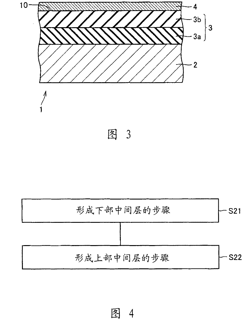
[0061] Figure 7 The structure of the shown superconducting wire 1 is basically the same as image 3 The superconducting wire rod shown is similar, except that the surface to be ground 10 is formed on the upper surface of the lower intermediate layer 3a in the intermediate layer 3 instead of the upper surface of the upper intermediate layer 3b in the intermediate layer 3, and the ground The upper surface of the substrate 2 is used to form the polished surface 20 . The superconducting wire rod 1 constituted in the above manner can also be provided with image 3 A similar effect is shown for the superconducting wire 1 . In addition, since the upper surface of the substrate 2 is also the flattened surface 20 to be polished, the flatness of the upper surface of the intermediate layer 3 can be further improved. Therefore, the in-plane orientation of superco...
PUM
| Property | Measurement | Unit |
|---|---|---|
| surface roughness | aaaaa | aaaaa |
| thickness | aaaaa | aaaaa |
| thickness | aaaaa | aaaaa |
Abstract
Description
Claims
Application Information