Supercharge Your Innovation With Domain-Expert AI Agents!

Display motherboard, display panel and manufacturing method thereof, and display apparatus

a display motherboard and motherboard technology, applied in non-linear optics, instruments, optics, etc., can solve the problems of sealant puncture, sealant breakage, and many undesirable phenomena of display panels

Active Publication Date: 2018-07-03
BEIJING BOE OPTOELECTRONCIS TECH CO LTD +1
View PDF17 Cites 0 Cited by
  • Summary
  • Abstract
  • Description
  • Claims
  • Application Information

AI Technical Summary

Benefits of technology

The present disclosure provides a display motherboard, panel, and manufacturing method, as well as a display apparatus, which avoids issues such as sealant puncture and breakage after cutting with sealant. The display motherboard has a blocking wall that prevents sealant from leaking out of the cutting line, ensuring a wider sealant width after curing. This improves the reliability and robustness of the display panels during assembly and testing.

Problems solved by technology

Upon using this method, since the sealant at the edges of a display panel is not blocked by the sealant for an adjacent display panel, the sealant at the edges of the display motherboard would spill from the display panels in considerable amount when the sealant is fittingly pressed and cured, such that the width of reserved sealant within the display panels after the curing becomes smaller, and accordingly, many undesirable phenomena arise from the display panels after the cutting with sealant, like sealant puncture, sealant break and so on, which could not be approved during such tests as Peel-off, Bending, etc.

Method used


Image

  • Display motherboard, display panel and manufacturing method thereof, and display apparatus
  • Display motherboard, display panel and manufacturing method thereof, and display apparatus
  • Display motherboard, display panel and manufacturing method thereof, and display apparatus

Examples


Embodiment Construction

[0030]The implementation of the present disclosure will be further illustrated below in conjunction with the accompanying drawings. The embodiments below are used only for making clearer illustration of the technical solution of the present disclosure rather than for limiting the scope of the present disclosure.

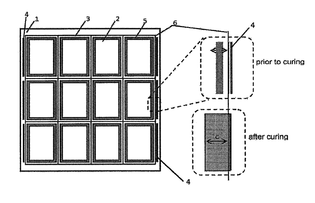
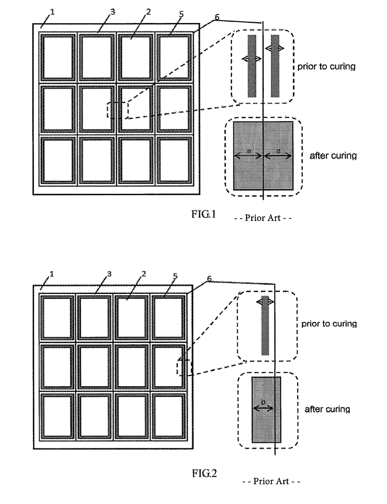
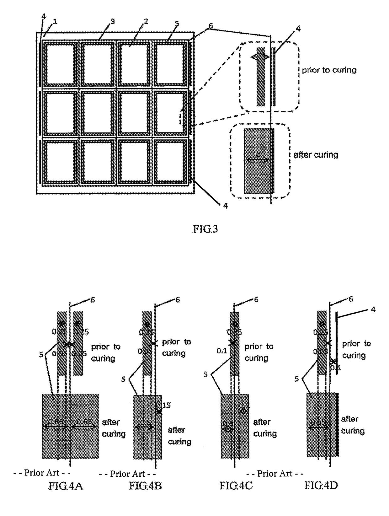
[0031]When the panel cutting in a liquid crystal display panel adopts cutting with sealant, a coating of an uncured sealant 5 is applied around the display panel 2, and then cell assembling is performed between an upper and a lower substrate 1. During the cell assembling, the sealant would be extruded to scatter sideways. FIG. 1 shows a schematic diagram of the sealant, prior to and after being cured, for adjacent display panels in a display motherboard 3 according to the prior art. As shown in FIG. 1, for the display panels located intermediately on the display motherboard 3, the sealant 5 in the adjacent display panels would function as a block to each other when it spills ...


PUM

PropertyMeasurementUnit
widthaaaaaaaaaa
widthaaaaaaaaaa
distanceaaaaaaaaaa

Abstract

The present disclosure describes a display Q_panel, a display panel and a manufacturing method thereof, as well as a display apparatus. The display Q_panel comprises a first and a second substrate for cell assembling to pre-form a plurality of display panels. The display Q_panel is provided, between the first substrate and the second substrate, with a blocking wall at the edge region on at least one side thereof, the blocking wall being located externally to the outmost cutting line on that side where it is located, and the sealant on that side being provided internally to the blocking wall. By providing a blocking wall externally to the outmost cutting line on the display Q_panel, the blocking wall blocks the spill-out of the sealant on that side, reduces the undesirable phenomena of sealant puncture, sealant break, etc. arising from the display panels after the cutting, can respond better to the Peel-off, Bending or other tests, and improves the robustness of glass cell assembling.

Description

RELATED APPLICATIONS[0001]The present application claims the benefit of Chinese Patent Application No. 201510103673.4, filed Mar. 9, 2015, the entire disclosure of which is incorporated herein by reference.TECHNICAL FIELD[0002]The present disclosure relates to the field of display technology, and specifically to a display motherboard, a display panel and a manufacturing method thereof, as well as a display apparatus.BACKGROUND ART[0003]The Liquid Crystal Displays (LCD) enjoy a number of advantages such as being light and slim, compact and small, and low in power consumption and heat generation, and so on. These advantages have caused LCDs to emerge from various types of display apparatuses and be widely used in modernized information equipment including TV sets, computers, tablet PCs, mobile phones, etc.[0004]Currently, with constant growth of the flat-panel display technology, consumers are driven gradually to switch their attentions to the appearances and the diversified functions...

Claims


Application Information

Patent Timeline
Patent Type & Authority Patents(United States)
IPC IPC(8): G02F1/1333G02F1/1339
CPCG02F1/133351G02F1/1339G02F1/13394
Inventor XIAO, WENJUNCHEN, XIAOCHUANWANG, SHIJUNWANG, LEIJIANG, WENBOXUE, YANNALI, YUEBAO, ZHIYINGLV, ZHENHUAZHANG, YONGWANG, CHUNLEI
Owner BEIJING BOE OPTOELECTRONCIS TECH CO LTD
Features
  • R&D
  • Intellectual Property
  • Life Sciences
  • Materials
  • Tech Scout
  • Unparalleled Data Quality
  • Higher Quality Content
  • 60% Fewer Hallucinations
Learn More